AN170 - 直流开关电源的直接结温测量

设计人员常常需要测量直流开关电源的结温,这在温度试验箱中极难实现。如果采用热像仪,不仅精度不高,而且它在高温环境下很容易损坏;而外部温度传感器则很难固定到小尺寸封装上。本应用说明将通过演示帮助读者了解一种测量 IC 结温的实用方法,它通过电源正常 (PG) 引脚的 MOSFET 体二极管实现温度的直接读取。该方法直接读取电压,并利用了二极管电压与温度之间的关系。
简介
测量最大指定负载和环境温度下的结温对很多应用都非常重要。无论是低成本的批量产品,还是安全或生命维持应用,各行各业对了解器件结温以及确定温度极限在哪里都颇感兴趣。
本文将以MPS的MPQ4572为例进行说明。图 1显示了该器件的直流模块框图,其中包含了PG 体二极管。

图1: MPQ4572中的PG N沟道MOSFET 体二极管
MPQ4572是一款全集成固定频率同步降压变换器。它在峰值电流控制模式下可实现高达 2A 的连续输出电流。该器件支持 4.5V 至 60V 的输入电压范围,可适应各种降压应用。它通过 PG 引脚上的体二极管(MOSFET 的一部分)提供1mA正向电流源(见图 1)。
我们可以通过EVQ4572-QB-00A评估板测量二极管电压与温度之间的关系曲线(见图 2),也可以直接在定制板上测量;因为二极管的曲线特性取决于温度,与 PCB 的尺寸无关。
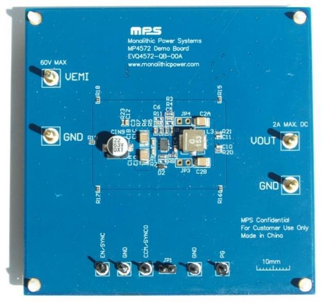
图 2:EVQ4572-QB-00A 4 层评估板 (8.9cmx8.9cm)
设计流程
电源正常 (PG) 引脚内包含一个带体二极管的内部 N 沟道 MOSFET。要精确测量结温,请按照以下步骤校准正向二极管电压和温度:
- 将PG 引脚上的任何电阻、微控制器或其他部件都断开。
- 将温度传感器(例如小型4 线PT1000)粘在被测器件封装的顶部。
或者在被测器件附近焊接一个浮动热电偶(建议将其焊接到 GND)。将温度传感器固定到封装上是一项艰巨的任务,因此请使用尽可能小的传感器,不要把温度传感器当作小型封装的散热器。用导热胶将 PT1000 温度传感器固定在封装上,或将热电偶直接焊接到电路板上具有 EMC 静电势(例如 GND 或 VIN)的部位(见图 3)。
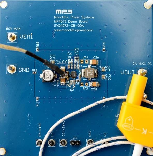
图 3:将热电偶焊接在PCB上
- 将具有内置二极管测试功能的精密万用表和1mA 电流源连接到PG 引脚(见图1和图5)。可以使用较小的电流,但必须与系统校准和测量时采用的电流相同。
- 在气候室中测量正向二极管电压与结温的关系。
- 用低于所需输入电压(VIN)的电源电压为器件供电,测量二极管电压。确定哪些VIN值具有有效校准值;因为VIN会影响效率,从而影响器件温度。DC/DC 变换器输出端不能连接负载。
- 在评估板上或定制PCB上进行测量。
- 关断器件。
- 启动气候室(例如,温度为25°C),并确保外部温度传感器显示稳定的读数。
- 短暂启动器件并读取万用表上的电压。空载时的结温不应大幅升高,因为结中的功耗很低(只有几毫瓦)。 如果可能,请采用高级异步模式 (AAM);因为在这种模式下,小负载的静态电流较低。
- 关断器件。
- 将气候室温度设置为下一个选定的温度,让 PCB 温度稳定约 20 至 30 分钟(具体时长取决于 PCB 的比热容和尺寸)。
- 短暂启动器件并读取万用表上的电压。
- 再次关断器件。继续将气候室温度设置为下一个选定的温度。
- 在最大期望负载和最大环境温度下测量正向二极管电压。
注意事项
测量PG正向电压二极管时,需注意以下几点:
- 校准电压与结温的斜率几乎为线性。为获取最高精度,可使用更多测量点和多项式拟合函数。同时检查校准的可重复性。
- 同类器件具有相似的斜率,但通常具有不同的偏移量。
- 相似器件通常斜率会略有不同。
- 可能会产生副作用,例如VOUT产生微小变化。但这不应被视为故障,因为结内的耦合电流也会产生此类影响。
- 这种测量方法的主要优势在于,可利用正向二极管电压来计算任意负载下的结温。
- 无需温度传感器。
- 请注意,并非所有元件都可使用PG 引脚来测量电流;请联系元件制造商获取产品指南。
测得的校准曲线
图 4显示了一个一阶 PG 正向二极管电压与结温之间的关系,它具有线性拟合函数关系。PG 二极管由图 1所示的外部 1mA 电流源驱动。

图 4:EVQ4572-QB-00A 上测得的校准曲线
通过测得的二极管电压,可使用公式 (1)计算结温:
$$voltage(T_{J})=-0.8068 \space x\space T_{J}\space x \space \frac {mV}{ºc} + 592.88mV $$体二极管读数与热像仪数据的比较
表 1 直接比较了结温读数和可视热像仪读数。环境温度通过铂电阻温度传感器 PT1000(28.0°C时阻值为1109Ω)测量。
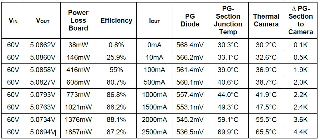
表 1:PG 正向二极管温度读数与热像仪读数的比较
从表 1可以看出,封装 PG 二极管部分的测得结温与热像仪温度相当。热像仪方法温度稍低,这是由结和封装顶面之间的模塑封料热阻导致的。可将热像仪发射率调整为 0.95,以适应封装的模塑料。组件之间的结温通常是不一致的,例如芯片内的 PG 部分温度就低于 MOSFET 部分。图 5为 PG 二极管部分和 MOSFET 部分示意图。

图 5:MPQ4572 封装内的MOSFET部分和 PG部分
不同电流负载下的温度测量
如图5和图10所示,小信号部分和功率MOSFET部分处于不同的位置。PG 正向电压二极管测量 PG 位置的结温,因此二极管温度一定与该位置的热像仪温度相当。而 MOSFET 的温度通常要高几度,因此需要将这个小偏移量添加到最大结温中。图6至图13显示了对应于表 1的热像仪测量值(均使用 EVQ4572-QB-00A 测量)。

图 6:ILOAD = 0mA 时的测量值

图 8:ILOAD = 100mA 时的测量值

图 10:ILOAD = 1000mA 时的测量值

图 12:ILOAD = 2000mA 时的测量值

图 7: ILOAD = 10mA 时的测量值

图 9:ILOAD = 500mA 时的测量值

图 11:ILOAD = 1500mA 时的测量值

图 13:ILOAD = 2500mA (1) 时的测量值
说明:
1)不建议采用连续 2.5A 电流。
应用
失效模式与影响分析 (FMEA)
失效模式与影响分析 (FMEA) 是一种对完整系统中的组件与子系统进行检查的方法。其目的是识别潜在的失效模式及其影响和原因。每个组件都使用预先定义的流程进行测试,以模拟失效组件或超出其标称规格的组件。每个失效组件都会影响整个系统的实效模式。通过了解这些失效模式带来的影响,设计人员可以确定所选组件是否会导致系统精度下降,或者是否会对用户或环境带来潜在危险。
通过上述方法直接测量结温,即使在困难的工作条件下,设计人员也可以轻松获得结温的准确测量值。直流开关电源的结温通常是 PCB 上最热的区域,其测量值对 FMEA非常有用。
高加速寿命试验 (HALT)
高加速寿命试验 (HALT) 是一种用来提高产品可靠性的测试,它广泛应用于多种行业,包括电子、医疗、计算机、汽车和军事等。HALT 测试通常在组件或系统指定的最高工作温度和机械振动水平之外进行,用于深入了解系统的行为。
例如当直流开关电源的温度超过其指定的最大结温时,通过直接测量结温,用户可以快速了解器件是否能在其极限范围之外运行。HALT可以帮助探索系统中未被确认的未知数,为确认组件失效时的确切温度提供关键信息。
高加速应力筛选 (HASS)
高加速应力筛选 (HASS) 是一种有效的生产筛选法,用于查找产品中的制造缺陷。其目标是在产品生命周期中的生产阶段加速发现制造缺陷,以降低相关失效率。
结语
在无法使用热像仪的温箱中,直接温度读取法简化了设计工程师测试定制 PCB 的过程。这种方法可以获得快速、可靠和精确的结温数据,无需复杂且通常耗时的过程,例如将温度传感器固定在器件封装上。
直接登录
创建新帐号