利用数字 PWM 信号调整 ICC 的实现方法

1 概述
1.1 简介
很多现代电子设备都需要多个电池供电,如工业医疗设备、扫地机器人、无人机和大功率扬声器等。其中一些设备还需要能够实时调整充电电流,以调节设备在不同操作模式下的性能。例如,许多电池制造商要求不同温度下的充电电流达到特定水平以保证电池安全。MP2759 提供 JEITA 配置以调节充电电流,并且可以通过微控制器 (MCU) 来增强用户配置。
本参考设计展示了一种通过来自 MCU 的 PWM 信号实时调整充电电流的方法。该设计采用了MPS高度集成的开关充电IC——MP2759,该器件专为1 节至 6 节串联锂离子或锂聚合物电池组应用而设计。
1.2 功能特性
- 高达 36V 的工作输入电压
- 高达 3A 的充电电流
- 支持1 节至 6 节电池串联,每节电池具有 3.6V、4.0V、4.1V、4.15V、4.2V、4.35V 或 4.4V 电池调节电压
- 输入电流限制调节
- 最小输入电压调节
- 支持“或”选择电源路径管理
- 0.5% 电池调节电压精度
- 充电操作指示
- 输入状态指示
- 电池过压保护(OVP)
- 充电安全定时器
- 使用 JEITA 配置的电池过温监控与保护
1.3 应用
- 工业医疗设备
- 电动工具
- 机器人和便携式真空吸尘器
- 无线扬声器
2 参考设计
2.1 功能框图
图 1 显示了一个高度集成的开关充电IC,用于 1 节至 6 节串联锂离子或锂聚合物电池组应用。该解决方案可提供 40W 输出功率,支持最大 36V 输入电压,并可通过外部 PWM 信号实时调节充电电流。
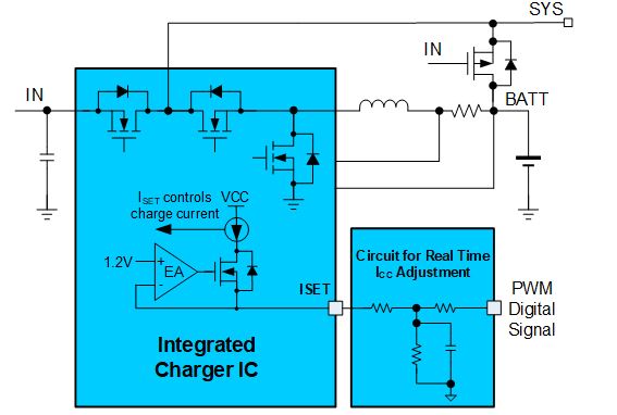
图1: 功能框图
2.2 相关解决方案
本参考设计基于以下 MPS 解决方案:
| MPS IC | 描述 |
| MP2759 | 带电源路径管理功能的 36V 开关充电器IC,适用于 1 节至 6 节电池 |
表1: 系统规格
2.3 系统规格
| 参数 | 规格 |
| 输入电压范围 | 4V 至 36V |
| 输出电压 | 高达 26.4V |
| 最大输出电流 | 3A |
| 开关频率 | 700kHz 或 450kHz(标称条件下) |
| 效率 | >92% |
表2: 系统规格
3 设计
3.1 设计过程
图 2显示了一个可为多个电池充电的应用电路。该电路可通过电源路径管理功能实时调节充电电流。其功率级包含一个电感(L1)和三个电容(CIN、CPMID 和 CBATT)。通过添加适当的外部元件,可实现带电源路径管理的完整充电功能。
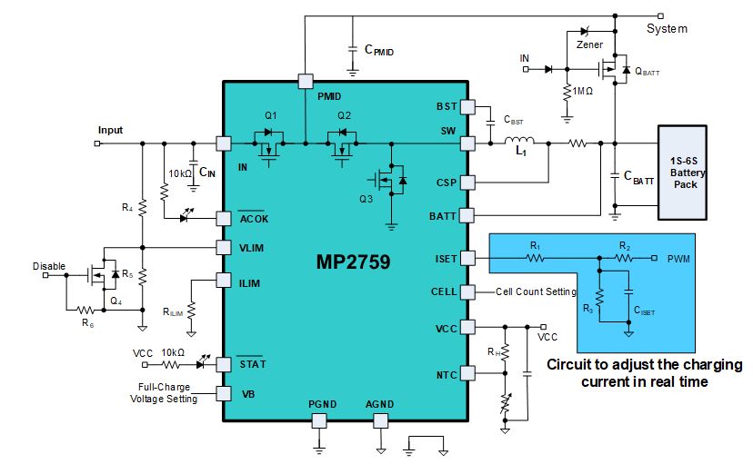
图2: 应用电路
MP2759提供了调节充电电流的功能,该功能通过在 ISET 引脚和 AGND 之间连接一个电阻器(RISET)来实现。ISET 引脚上的电压固定在 1.2V 左右。RISET与充电电流之间的关系可以用公式(1)来表示:
$$I_{CHG}= \frac {96(k\Omega)}{R_{ISET}(k\Omega)}$$图 3所示为等效 RISET电路。通过修改MCU 的 PWM 信号占空比,可更改等效RISET值。这意味着充电电流可实时调节。
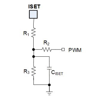
图3: 等效 RISET 电路
3.4 PCB 布局
参看图 5、图 6、图 7 和图 8中的 PCB 布局以了解标准的 MP2759 评估板。
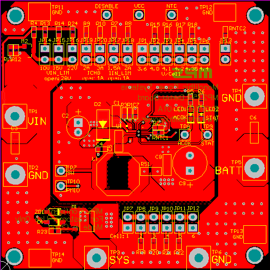
图5: 顶层
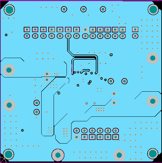
图7: 中间层2
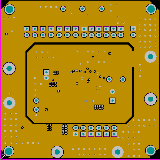
图6: 中间层1
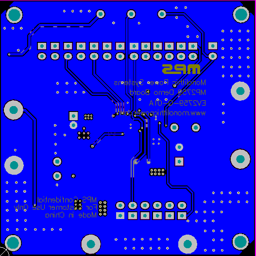
图8: 底层
4 测试结果
4.1 效率
测试条件:L = 10µH/35mΩ,fSW = 700kHz,RSNS = 20mΩ,TA = 25°C.
恒压模式

图10: 效率与充电电流
4.3 散热测量
测试条件:L = 10µH/35mΩ,RSNS = 20mΩ,fSW = 700kHz,TA = 25°C,工作 20 分钟。电路板信息:63.5mmx63.5mm,4层,1盎司/层。
VIN = 36V,VBATT = 24V,ICC = 2A,
TRISE = 从67.3°C 降至 25°C = 42.3°C
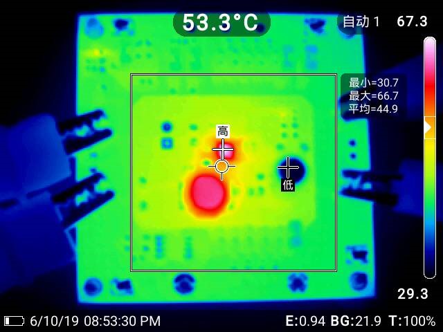
图27: 热成像
VIN = 16V,VBATT = 12V,ICC = 3A,
TRISE = 从70.8°C 降至 25°C = 45.8°C
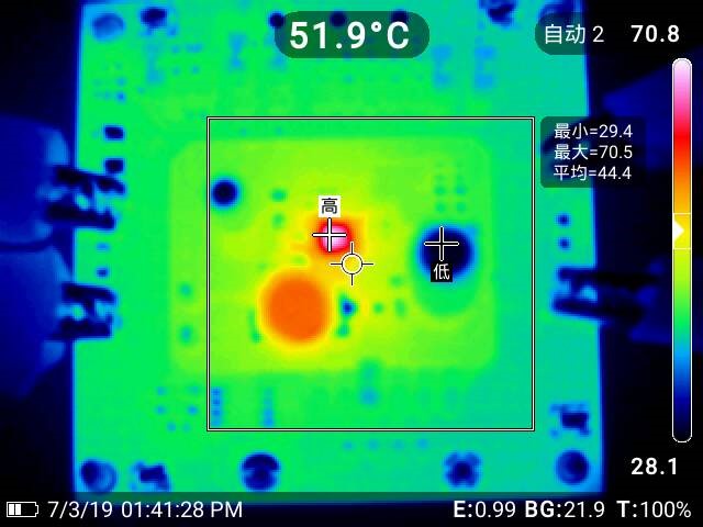
图28:热成像
直接登录
创建新帐号