Trace Routing and Placement
It is essential to ensure electromagnetic compatibility (EMC) and minimize electromagnetic interference (EMI) by ensuring that trace routing and placement on printed circuit boards (PCBs) are done correctly. The arrangement of traces has an impact on the quality of the signals, the amount of noise that is produced, and the overall performance of electrical circuits. The purpose of this part is to investigate the most effective methods for trace routing and placement in order to improve EMC performance.
Key Principles of Trace Routing and Placement
Short and Direct Traces:
Minimize Length: Keeping signal traces as brief and direct as feasible is an important part of minimizing length. It is possible for longer traces to function as antennas, with the ability to radiate and gather up undesired electromagnetic radiation.
Direct Paths: In order to ensure signal integrity and decrease the possibility of electromagnetic interference (EMI), it is recommended to make use of direct pathways for key signal lines. This will assist in reducing inductance and resistance.
Differential Pair Routing:
Matched Lengths: When routing differential pairs, for example, for high-speed data lines like USB or DDR memory signals, it is important to make sure that the traces are of similar length in order to preserve the integrity of the signal. Consequently, skew and differential-to-common mode conversion are reduced to a minimum.
Close Proximity: In order to improve the rejection of common-mode noise, route differential pairs in close proximity to one another. All of this contributes to the reduction of radiated emissions and helps to cancel out noise.
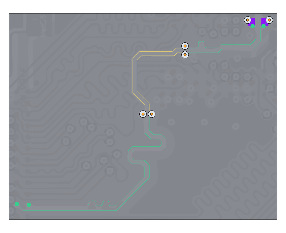
Figure 2: Example of Differential and Length Matched Signal Pair
Controlled Impedance:
Impedance Matching: When designing traces for high-speed signals, impedance matching involves designing lines with regulated impedance in order to reduce reflections and significant deterioration. With the use of impedance calculators and according to the recommendations provided by the PCB manufacturer, you may obtain the appropriate impedance.
Consistent Width: The impedance of a signal trace may be altered by altering its width, which is referred to as consistent width. To guarantee that the impedance remains continuous across the whole length of the trace, it is important to maintain a consistent trace width and spacing.
Separation of Signal Types:
High-Speed vs. Low-Speed: Separate high-speed signal traces from low-speed and analog traces. High-speed traces should be kept separate from low-speed traces. It is possible for high-speed signals to produce noise, which can cause interference with analog circuits that are sensitive.
Power and Signal Separation: The separation of power and signal traces is important because it helps to lessen the likelihood of coupling and interference by keeping power traces and high-current traces apart from signal traces.
Avoiding Right Angles:
Smooth Transitions: It is important to steer clear of right-angle bends when routing traces for high-speed signals since these bends might result in impedance discontinuities and increase radiated emissions. If you want to make transitions that are smoother, use angles of 45 degrees or curved traces.
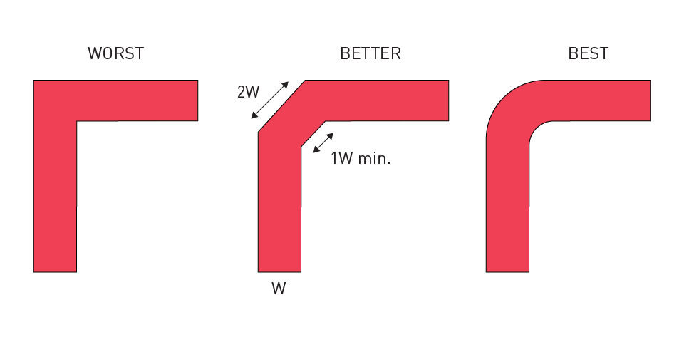
Figure 3: Trace Bending Practice for High-Speed Signals
Gradual Bends: This reduces the likelihood of signal reflection and improves signal integrity.
Ground and Power Planes:
Ground Return Paths: Make sure that the signal traces have a return path that is well-defined and uninterrupted on the ground plane that is next to them. This reduces EMI and minimizes the loop area.
Power Plane Considerations: Make use of power planes in order to decrease noise and distribute power in an equitable manner. In order to produce plane capacitance between the ground planes and the power planes, which helps further filter high-frequency noise across the printed circuit board (PCB), place the power planes near the ground planes.
Via Usage:
Minimize Vias: High-speed signal lines should minimize the use of vias as they can contribute to inductance and compromise signal integrity. When necessary, use multiple vias to reduce impedance.
Via Placement: When placing vias, it is important to do so with caution in order to guarantee that return current pathways are retained and that signal integrity is maintained.
Crosstalk Reduction:
Trace Spacing: By increasing the distance between parallel signal traces, also known as trace spacing, one can reduce capacitive coupling and crosstalk. Crosstalk is reduced to a lesser extent when the spacing is increased. It is recommended that the spacing between two parallel traces be at least twice as wide as the width of the traces. This is a general rule of thumb.
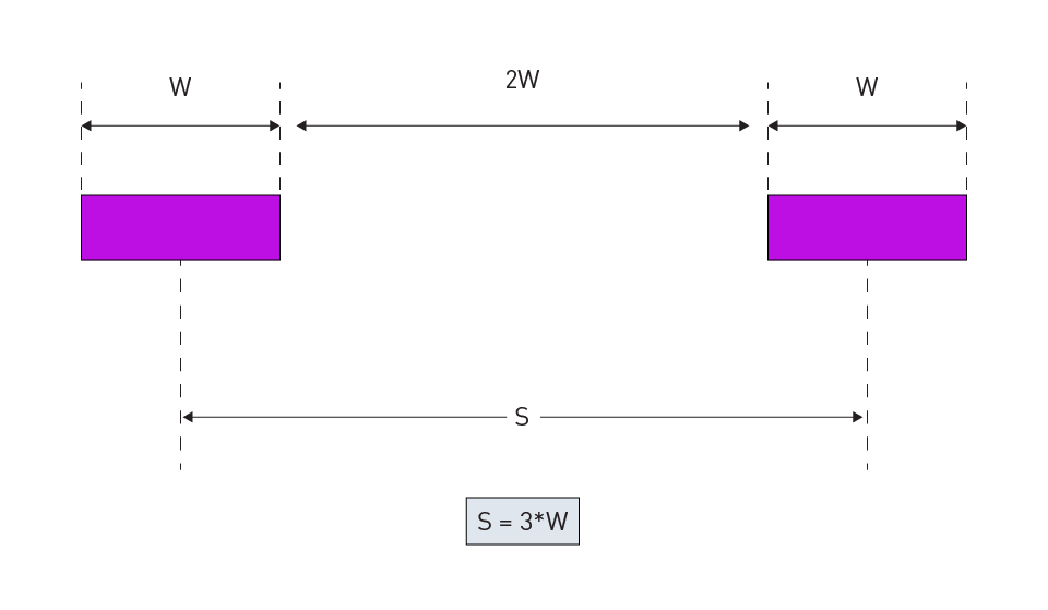
Figure 4: Trace Spacing Rule
Ground Traces: Inserting ground traces, also known as guard traces, between high-speed signal traces to further reduce crosstalk and improve signal integrity is a practice that is not widely known.
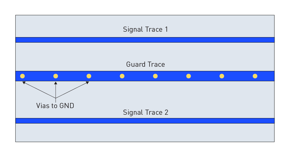
Figure 5: Ground as Guard Trace
Practical Examples and Techniques
High-Speed Digital Circuits:
Microstrip and Stripline: For high-speed digital traces, it is recommended to use either microstrip or stripline designs in order to manage impedance and decrease electromagnetic interference (EMI). On the other hand, stripline traces are located between two ground planes in the inner layers, whereas microstrip traces are located on the outer layers and have a ground plane beneath them. Utilize impedance calculators to align the trace impedance with the desired value.
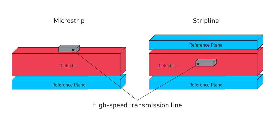
Figure 6: Microstrip and Stripline routing
Serpentine Routing: When it comes to high-speed differential pairs, serpentine routing is essential for providing length matching. This method ensures concurrent arrival of signals, thereby reducing skew.
Analog and Mixed-Signal Circuits:
Analog-Digital Separation: Ensure that the ground planes of the analog and digital components of the printed circuit board (PCB) are kept distinct. In order to prevent ground loops and to lessen the amount of noise coupling, connect these planes at a single intersection.
Shielding: In order to provide shielding, sensitive analog traces should be routed away from loud digital traces, and shielding should be provided appropriately. Use guard traces or metal shields to secure critical signals.
RF and Microwave Circuits:
Controlled Impedance Lines: When designing RF and microwave traces, it is important to apply the right transmission line methods in order to achieve controlled impedance. Ensure that both the substrate material and the trace shape can support the desired impedance.
Grounded Coplanar Waveguide: The use of grounded coplanar waveguide constructions for radio frequency (RF) traces is recommended in order to decrease radiation and restrict electromagnetic fields.
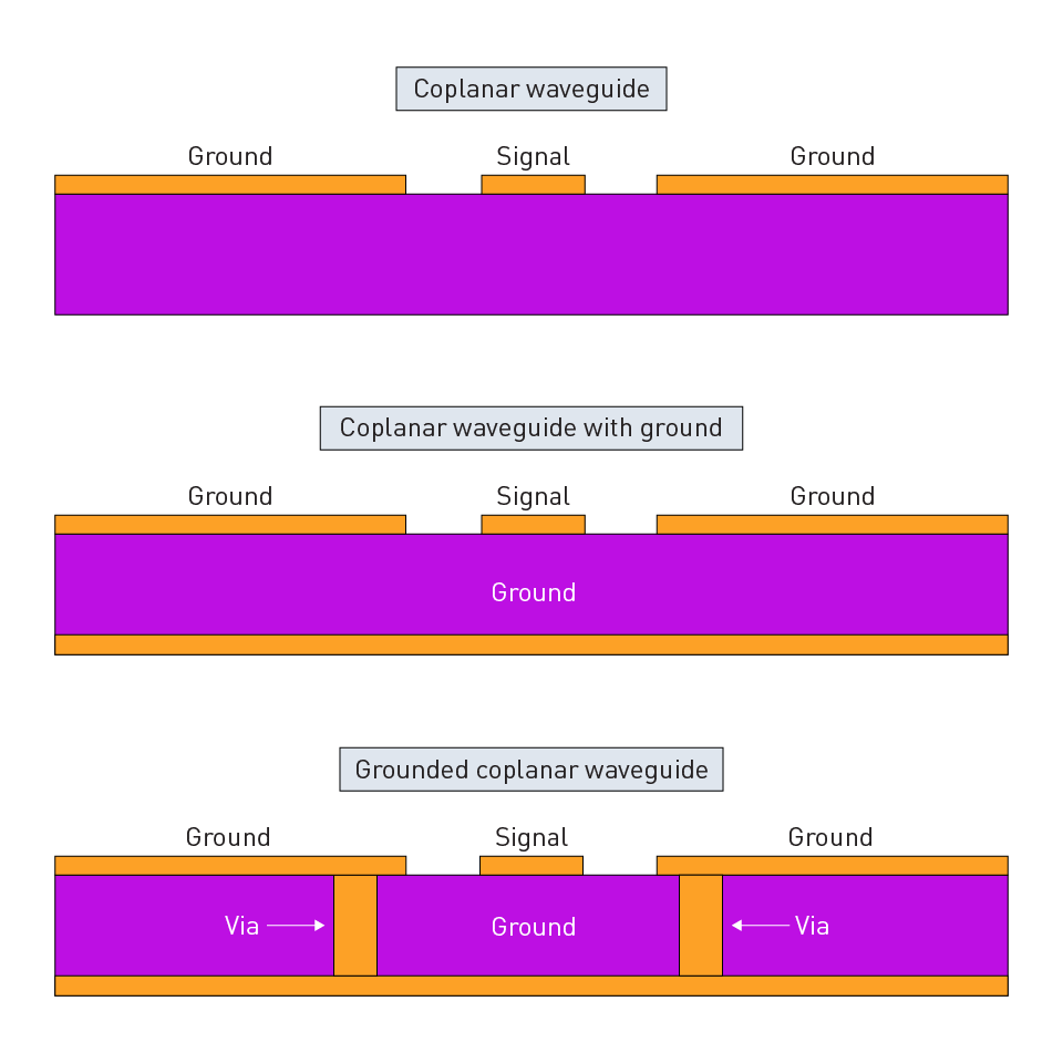
Figure 7: Different Solutions for Coplanar Waveguide
Testing and Validation
Signal Integrity Analysis:
Simulation Tools: To examine and optimize trace routing, you need to make use of signal integrity simulation tools. Reflections, crosstalk, and impedance mismatches are some of the possible problems that may be identified with the use of these instruments.
Time-Domain Reflectometry (TDR): Carry out TDR measurements in order to validate the impedance of high-speed traces and identify discontinuities.
Pre-Compliance Testing:
EMI Scans: Pre-compliance electromagnetic interference (EMI) scans should be carried out in order to locate and eliminate sources of radiated and conducted emissions. Assessing the efficiency of trace routing and placement may be accomplished through the utilization of spectrum analyzers and near-field probes.
Iterative Testing: In order to guarantee that the final design satisfies EMC criteria, it is necessary to do iterative testing and revise the PCB layout depending on the results of the tests.
Layer Stacking and Power Plane Management
When it comes to printed circuit board (PCB) design, layer stacking and power plane management are two essential components that have a substantial influence on the performance of electromagnetic interference (EMI) and overall electromagnetic compatibility (EMC). It is possible to decrease noise, improve signal integrity, and limit electromagnetic interference (EMI) by properly configuring layer stacks and power planes. In order to maximize the effectiveness of EMC, this section goes into the most effective methods for layer stacking and power plane control.
Key Principles of Layer Stacking
Layer Count and Configuration:
Multilayer PCBs: Use multilayer printed circuit boards (PCBs) to efficiently regulate signal integrity and electromagnetic interference (EMC). More layers make it possible to have distinct ground and power planes, which in turn reduces electromagnetic interference (EMI).
Standard Configurations: Four-layer, six-layer, and eight-layer printed circuit boards are examples of common configurations. Both the intricacy of the design and its needs will determine the option.
Ground and Power Planes:
Dedicated Planes: In order to allocate dedicated layers for ground and power aircraft, dedicated planes should be assigned. As a result, impedance is reduced, and stable reference planes for signals are brought into existence.
Adjacent Layers: Creating a low-inductance decoupling capacitance may be accomplished by placing ground and power planes on different layers that are next to one another. This improves EMC and reduces high-frequency noise.
Signal Layer Arrangement:
Signal-Ground Pairs: In order to create signal-ground pairs, signal layers should be positioned next to ground planes. Because of this layout, the loop area is decreased, and the radiation from signal traces is reduced as well.
Power-Ground Sandwich: The common stack-up for a four-layer printed circuit board (PCB) is Signal-Ground-Power-Signal. There are many signal layers that are placed between the ground plane and the power plane in 6-layer and higher applications.
Example Layer Stacks
4-Layer PCB:
- Layer 1: Signal
- Layer 2: Ground
- Layer 3: Power
- Layer 4: Signal
6-Layer PCB:
- Layer 1: Signal
- Layer 2: Ground
- Layer 3: Signal
- Layer 4: Power
- Layer 5: Ground
- Layer 6: Signal
Key Principles of Power Plane Management
Power Plane Segmentation:
Separate Planes: In order to reduce noise coupling across power domains, it is recommended to make use of distinct power planes for each of the different voltage levels. Every power aircraft needs to be situated in close proximity to a ground plane.
Decoupling Capacitors: Position decoupling capacitors in close proximity to the power pins of integrated circuits (ICs) in order to maintain levels of voltage stability and eliminate noise. Ensure that capacitors are distributed uniformly throughout the power plane.
Plane Isolation and Stitching:
Stitching Vias: Utilize stitching vias to link several ground planes, therefore lowering impedance and enhancing current return routes. Stitching vias are also known as sewing vias. This is of utmost significance in matters pertaining to high-frequency designs.
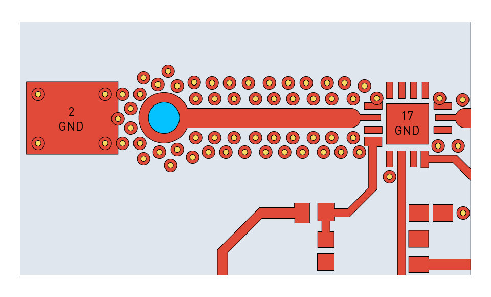
Figure 8: Stitching Vias
Isolated Islands: Because isolated islands can function as antennas and broadcast electromagnetic interference (EMI), it is important to avoid producing them in power and ground planes. The planes should be continuous, and the vias should be well linked.
Ground Plane Management:
Solid Ground Planes: In order to offer a constant reference for signals and to prevent electromagnetic interference (EMI), it is recommended to make use of solid ground planes rather than divided or partial planes.
Multiple Ground Planes: When designing multilayer infrastructures, it is important to make use of several ground planes in order to further improve signal integrity and minimize noise. Ensure the proper linking of all the ground planes.
High-Frequency Design:
Decoupling Networks: Implementing a network of decoupling capacitors with different values (for example, 0.01 µF, 0.1 µF, and 1 µF) is necessary in order to span a wide frequency range with decoupling networks. Capacitance of varying values can successfully filter distinct wavebands before they become inductive.
Localized Decoupling: Place larger capacitors close to power entry points and smaller capacitors adjacent to individual integrated circuits in order to provide localized decoupling.
Mixed-Signal Design:
Analog and Digital Separation: Separation of Analog and Digital To reduce the amount of noise coupling, it is necessary to separate the analog and digital power planes. Ground loops can be avoided by connecting the analog and digital grounds at a single location, which is known as star grounding.
Decoupling and Filtering at the PCB Level
When it comes to the design of printed circuit boards (PCBs), decoupling and filtering are two approaches that are essential for reducing electromagnetic interference (EMI) and guaranteeing electromagnetic compatibility (EMC). These techniques contribute to the preservation of signal integrity, the reduction of noise, and the stabilization of power supply, which ultimately enables electronic systems to work more effectively overall. This section discusses numerous ideas and best practices for efficient decoupling and filtering at the printed circuit board (PCB) level.
Key Principles of Decoupling
Purpose of Decoupling:
Noise Reduction: Decoupling capacitors help filter out high-frequency noise from power supply, which in turn provides integrated circuits (ICs) with a voltage that is clean and stable.
Transient Suppression: In addition to having the ability to absorb transient voltage spikes, they also offer local energy storage, which guarantees that the integrated circuits will function without any power fluctuations.
Types of Decoupling Capacitors:
Bulk Capacitors: Bulk capacitors are utilized for the purpose of providing energy storage and maintaining voltage stability throughout a wide frequency regime. As a result of their high capacitance density, electrolytic or tantalum capacitors are typically utilized for the purpose of bulk decoupling.
Local (Bypass) Capacitors: IC power pins are located in close proximity to local (bypass) capacitors, which are used to filter high-frequency noise. Numerous applications frequently utilize ceramic capacitors with low equivalent series resistance (ESR) and inductance (ESL).
Placement and Value Selection:
Proximity to ICs: Position decoupling capacitors in such a way that they are as close as feasible to the power pins of integrated circuits (ICs) in order to reduce the inductance of the connecting traces and enhance the efficiency of the filtering process. Use numerous vias to connect the capacitor to earth through a low-inductance connection.
Multiple Values: Capacitors of varying values, such as 0.01 µF, 0.1 µF, and 1 µF, should be used in parallel to cover a wide frequency spectrum. This will ensure that noise suppression is effective throughout a wide range of frequencies.
Key Principles of Filtering
Purpose of Filtering:
EMI Suppression: Filters prevent undesired high-frequency noise from entering or exiting the printed circuit board (PCB), hence lowering both conducted and radiated emissions related to electromagnetic interference (EMI).
Signal Integrity: Filters contribute to the preservation of signal integrity by reducing noise from signal lines, which in turn improves the overall performance of the system through their removal.
Types of Filters:
Low-Pass Filters: When low-pass filters are used, they allow low-frequency signals to get through while attenuating noise that is of higher frequency. capacitors, inductors, ferrite beads, or a mixture of the two are frequently used in the implementation of this technology. There is a decent rule of thumb that states that the cut-off frequency of the filter should be placed one decade below the frequency of the noise that is of interest in order to reduce the noise by at least 20 dollars.
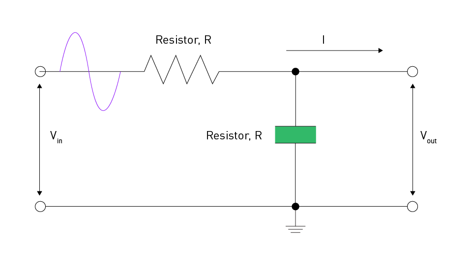
Figure 9: Example Resistor-Capacitor Low-pass Filter
Common-Mode Chokes: On differential signal lines, common-mode chokes are utilized for the purpose of suppressing common-mode noise. When it comes to common-mode signals, they offer a high impedance, but differential signals are able to flow through without any difficulties. Essentially, several transformers share a core that realizes two inductors. The common mode current generates an opposing magnetic field as it passes through both inductors.
Feedthrough Capacitors: Feedthrough capacitors are a form of capacitor that, in comparison to ordinary capacitors, offer a route to ground that has a reduced inductance. In the process of filtering noise with very high frequencies, they are utilized.
Implementation Techniques:
Power Line Filtering: The use of low-pass filters on power lines in order to suppress high-frequency noise is referred to as power line filtering. Using inductors in conjunction with capacitors can filter noise at lower frequencies; however, at frequencies higher than 100 MHz, one should use ferrite beads in conjunction with capacitors.
Signal Line Filtering: Install filters on signal lines, particularly those that are entering or leaving the printed circuit board (PCB). Whenever it is necessary, make use of common-mode chokes, capacitors, and series resistors.
Practical Techniques for Decoupling and Filtering
Decoupling Networks:
Distributed Decoupling: Decoupling Distributed: Distribute decoupling capacitors uniformly over the printed circuit board (PCB), making sure that each integrated circuit (IC) has sufficient local decoupling. In addition to enhancing noise suppression, this results in a reduction in the impedance of the power distribution network.
Power Plane Connection: The power plane connection involves connecting decoupling capacitors directly to the power and ground planes using short, broad traces and numerous vias. This is done in order to reduce the amount of inductance and resistance.
Filtering Strategies:
Pi Filters: For efficient power line filtering, use Pi filters, which are a configuration consisting of capacitors, inductors, and capacitors. There is low-pass filtering provided by this topology, which reduces the amount of high-frequency noise that is coming from both sides.
LC Filters: Combining inductors and capacitors results in the formation of LC filters, which may be used on both signal and power lines. Choose the values of the components depending on the cutoff frequency that you want to achieve and the characteristics of the noise that you want to eliminate.
A reasonable rule of thumb to follow when selecting the cut-off frequency for LC filters is to choose a frequency that is at least ten years lower than the frequency of the noise of interest.
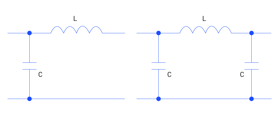
Figure 10: LC Filter and PI Filter Topology
The cut-off frequency of an LC filter can be calculated by the Thomson formula:
$$f_c = \frac{1}{2\pi\sqrt{LC}}$$Where:
Best Practices for Component Placement:
Proximity to Noise Sources: In order to prevent noise at its source, it is important to position filters in close proximity to noise sources. Some examples of noise generators are switching regulators and high-speed signal drivers. Wherever it is relevant, follow the advice on the datasheet.
Entry and Exit Points: Filters should be positioned at entrance and departure points of the printed circuit board (PCB) in order to prevent noise from traveling via connections and cables after they have been inserted.
Example Implementations
High-Speed Digital Circuits:
Decoupling Capacitors: Using numerous ceramic capacitors of differing values in close proximity to the power pins of microprocessors and high-speed digital integrated circuits is an effective method for decoupling capacitors. This guarantees that the decoupling happens effectively throughout a broad frequency range.
Power Line Filters: In addition to the LC filters that are used to provide high-speed circuits, power line filters should also be used to reduce high-frequency noise. Ferrite beads should be applied to power lines.
Analog and Mixed-Signal Circuits:
Local Decoupling: To preserve the integrity of the signal, it is necessary to position high-value ceramic capacitors in close proximity to the power pins of sensitive analog components, such as operational amplifiers and ADCs.
Signal Filtering: Use RC low-pass filters on analog signal lines for signal filtering to reduce high-frequency noise and improve the accuracy of analog measurements.
RF and Communication Circuits:
Broadband Decoupling: To complete the process of broadband decoupling, a combination of capacitors is necessary to span the entire frequency range that RF circuits operate at.
Common-Mode Chokes: On differential RF communication lines, common-mode chokes reduce noise from common-mode interference and enhance signal quality.
Testing and Validation
Frequency Response Analysis:
Network Analyzers: Network Analyzers Determine the frequency response of decoupling and filtering networks by employing network analyzers to assess the frequency response. In this way, the efficacy of the components and configurations that were chosen may be independently verified.
Impedance Analysis: When building high-speed circuits like DDR memory, it is important to do impedance analysis to verify that decoupling capacitors offer low impedance across the frequency range that is needed.
EMI Testing:
Conducted Emissions: Using line impedance stabilization networks (LISNs) and spectrum analyzers, conduct pre-compliance testing for conducted emissions. This testing is required for compliance with regulations. This helps detect possible sources of electromagnetic interference (EMI) and limit their effects.
Radiated Emissions: To be sure that the filtering and decoupling steps work to lower electromagnetic radiation, tests for radiated emissions must be done in echo-free rooms.
直接登录
创建新帐号