为汽车SoC电源树选择最佳PoL变换器

简介
汽车系统的算力需求不断攀升,对高级驾驶辅助系统(ADAS)和信息娱乐系统片上系统 (SoC) 的功率需求也水涨船高。SoC 可能需要独立的电源轨,电流范围从几百安到几毫安不等。本文将围绕汽车 SoC 的预稳压器设计,深入探讨如何完成复杂的最佳负载点 ( PoL ) 变换器选择,以实现SoC 电源轨供电。
片上系统 (SoC) 的电源需求
在讨论组件选型之前,我们先列出本案例的SoC电源需求(见表1)。
表1:SoC电源需求
| 电源轨名称 | 电压(V) | 电流(A) | 瞬态负载(A) | 斜率 (A/µs) | 电压容差(1) (%) | 注释 |
|---|---|---|---|---|---|---|
| VDD_CORE | 0.85 | 60 | 40 | 40 | 3 | |
| 1V8_GPIO | 1.8 | 5 | 2.5 | 2.5 | 5 | |
| 3V3_GPIO | 3.3 | 5 | 2.5 | 2.5 | 5 | |
| 1V8_analog | 1.8 | 1.5 | 0.75 | 0.75 | 5 | 来自低噪声 DC/DC 变换器 |
| DDR_VDD | 1.05 | 6 | 3 | 3 | 3 | |
| DDR_VDDQ | 0.6 | 6 | 3 | 3 | 5 | |
| PCIe | 0.85 | 1.5 | 0.75 | 0.75 | 5 | |
| MIPI | 0.75 | 1.5 | 0.75 | 0.75 | 5 |
注释:
1) 电压容差包括变换器的直流精度、负载瞬态响应和IR压降。
最大额定电流是上表中最重要的参数,它决定IC的选型。一方面,为确保最佳性能,DC/DC变换器的标称输出电流(IOUT)必须等于或大于电源轨的额定电流;另一方面,建议所选器件提供的电流不超过电源轨所需电流的150%,以实现最优性价比。基于这些考虑,能够满足系统要求的IC选择范围就已经缩小,然后,再考虑其他需求,进一步优化选择范围。
瞬态负载和电压容差对于器件的选择也起着重要的作用。如果瞬态负载变化较大(>额定电流的30%)且电压容差较小(<5%),则应选择具有出色负载瞬态响应的器件。这类器件通常采用恒定导通时间 (COT) 或零延迟 PWM (ZDP) 等先进控制方法(见图 1),因此具有超快负载瞬态响应,并能最大限度地降低输出电容要求,以满足容差要求。
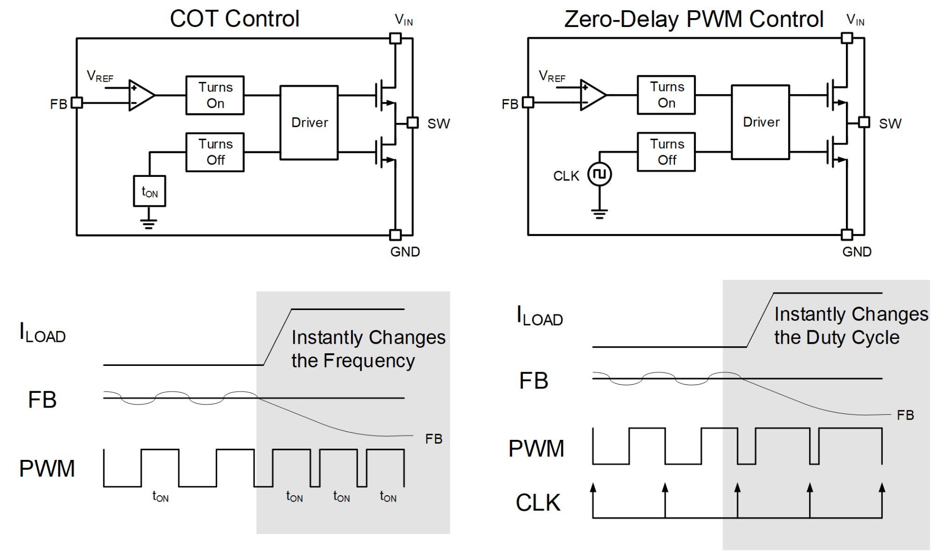
图1: COT 控制和ZDP控制
在注重成本及可扩展性的 ADAS 系统中,分立式PoL变换器因其高度灵活性而成为最佳电源方案。反之,电源管理 IC (PMIC) 将多个变换器集成到单个器件中,虽然简化了设计,但相对僵化,无法根据具体应用灵活定制。PoL器件则可以放置在 SoC 附近,有助于构建良好的电源传输网络。此外,由于变换器以热量的形式耗散能量,因此采用分立式 IC 可以分散热源,从而简化热管理。


为电源轨选择合适的部件
VDD_CORE 电源轨
首先看VDD_CORE电源轨,其最大额定电流为60A,要求相当高。我们可以采用多相稳压器 (VR) 控制器,例如MPQ2967-AEC1,来提供高电流和低输出电压(见图 2)。此外,VR 控制器需要与DrMOS配合使用,才能构建完整的电源变换器。DrMOS 为内置功率 MOSFET 和栅极驱动器的单片半桥器件。
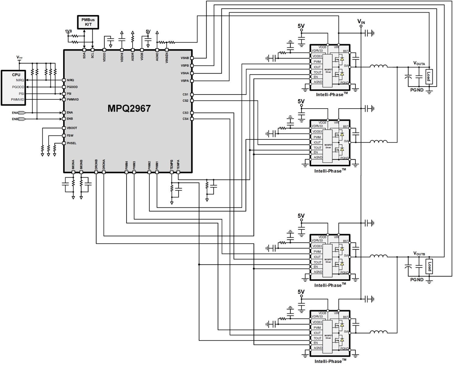
图 2: MPQ2967-AEC1 – 采用 Intelli-PhaseTM 架构的多相 VR 控制器
采用先进控制技术的汽车级控制器可最大限度地减少对电源轨的干扰,从而实现出色的瞬态响应性能。DrMOS也是高效紧凑的高负载解决方案。建议将MPQ2967-AEC1控制器与两个MPQ86960-AEC1 Intelli-PhaseTM IC 搭配使用,以实现可支持60A输出负载电流的双相变换器。
其余电源轨所需电流明显较低,因此可采用常规单片降压变换器,将5V总线电压转换为每个电源轨所需的电压。
1V8_GPIO 和3V3_GPIO电源轨
1V8_GPIO和3V3_GPIO电源轨均需5A电源电流,但其瞬态负载和电压容差规格较其他电源轨宽松。对此,选择高性价比的理想变换器就很关键,因为这有助于降低总体解决方案成本。MPQ2167A-AEC1 是一款非常适合这些电源轨的器件,它可以在紧凑的3mmx3mm封装中提供高达6A的输出电流。其2.2MHz的开关频率也使得采用更小体积、更低额定值的无源元件成为可能,从而节省成本和面积。该变换器还具有峰值电流模式(PCM)控制和内部补偿功能,性能稳定且能维持所需的电压调节能力。
1V8_analog、PCIe和MIPI 电源轨
为1V8_analog电源轨选择组件比较有挑战性,因为它要为 SoC 中要求稳定、低噪声电源的敏感模拟电路供电。而且它还需要1.5A的最大电流,对于低噪声低压差 ( LDO ) 线性稳压器来说,这是很高的要求。在环境温度可能高达85°C甚至更高的汽车环境中,这种LDO会出现过热情况。
高效率降压变换器,如MPQ2178-AEC1,非常适合1V8_analog电源轨,但其输出噪声必须衰减才能满足设计要求。在变换器输出端添加一个二级滤波器可以提供低噪声电源所需的衰减(见图 3)。SoC 硬件手册应就如何为这种电源轨设计滤波器提供指导,也可参考文章:如何设计低噪声电源的二级滤波器。
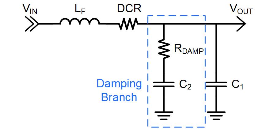
图 3:带阻尼支路的二级输出滤波器
MPQ2178-AEC1可以为低电流电源轨供电。这款器件采用先进的 COT 控制,在稳态下以恒定的2.4MHz开关频率(fSW)工作,并能提供出色的瞬态负载响应。
MPQ2178-AEC1可复用于 PCIe 和 MIPI 电源轨,因为这两个电源轨与1V8_analog轨需求类似,除了不需要二级输出滤波器。
DDR内存供电轨
最后,两个 DDR 内存供电轨均需要6A输出电流和出色的负载瞬态响应。DDR_VDD 电源轨的电压容差要求为 3%;在1.05V标称电源轨条件下,仅允许 ± 31.5mV 的偏差。
DDR_VDDQ电源轨的电压容差较高,为 5%。但0.6V的标称电压下仅允许30mV的偏差。此外,允许电压偏差中还要减去所选 IC 的直流精度,这使允许负载瞬变干扰的空间进一步缩小(图 4)。
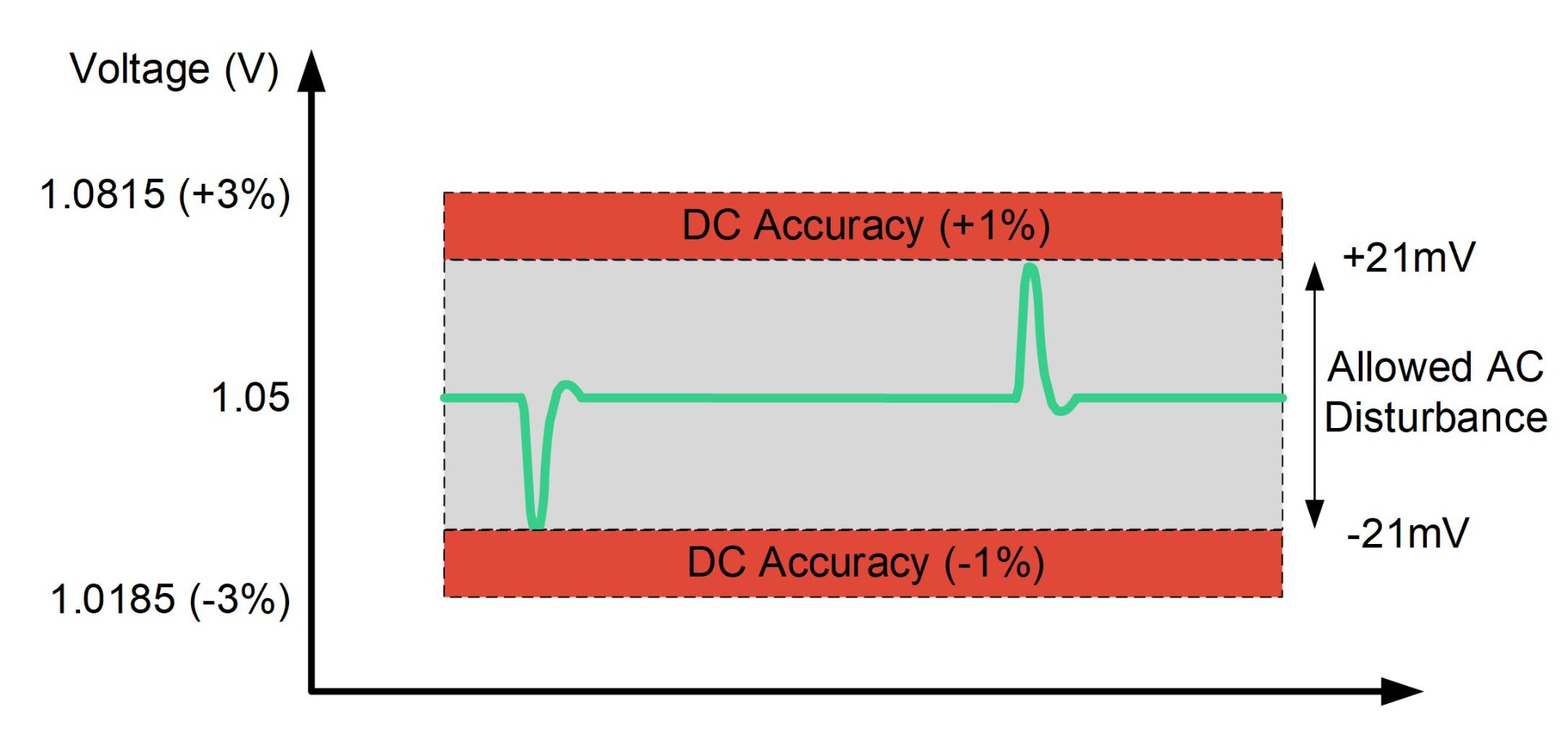
图 4:允许的交流干扰空间
选择一款在全工作范围内具有 1% 出色精度并具有快速控制环路的 IC 非常重要。作为一款先进的低压降压变换器,MPQ2283-AEC1专为满足这些严格的功率需求而设计。该器件采用ZDP控制环路,可实现快速瞬态响应,并能够以最小输出电容将电压扰动控制在 ±15mV以内。
器件选型总结
表 2 总结了针对本应用示例所选的器件。
表 2:所选器件列表
| 电源轨名称 | 电压(V) | 电流(A) | 产品型号 |
|---|---|---|---|
| VDD_CORE | 0.85 | 60 | MPQ2967GQKTE-AEC1 |
| 2 x MPQ86960GMJT-AEC1 | |||
| 1V8_GPIO | 1.8 | 5 | MPQ2167AGQE-AEC1 |
| 3V3_GPIO | 3.3 | 5 | MPQ2167AGQE-AEC1 |
| 1V8_analog | 1.8 | 1.5 | MPQ2178GQHE-AEC1 |
| DDR_VDD | 1.05 | 6 | MPQ2283GLE-AEC1 |
| DDR_VDDQ | 0.6 | 6 | MPQ2283GLE-AEC1 |
| PCIe | 0.85 | 1.5 | MPQ2178GQHE-AEC1 |
| MIPI | 0.75 | 1.5 | MPQ2178GQHE-AEC1 |
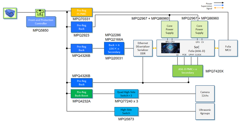
选定所有 IC之后,即可更新电源树以反映最终架构。之后,硬件工程师即可开始围绕所需无源元件开始计算工作,例如功率电感和输出电容。图 5 显示了最终的 SoC 电源树,该电源树经优化可满足所有电源轨的规格要求,包括预稳压器设计。
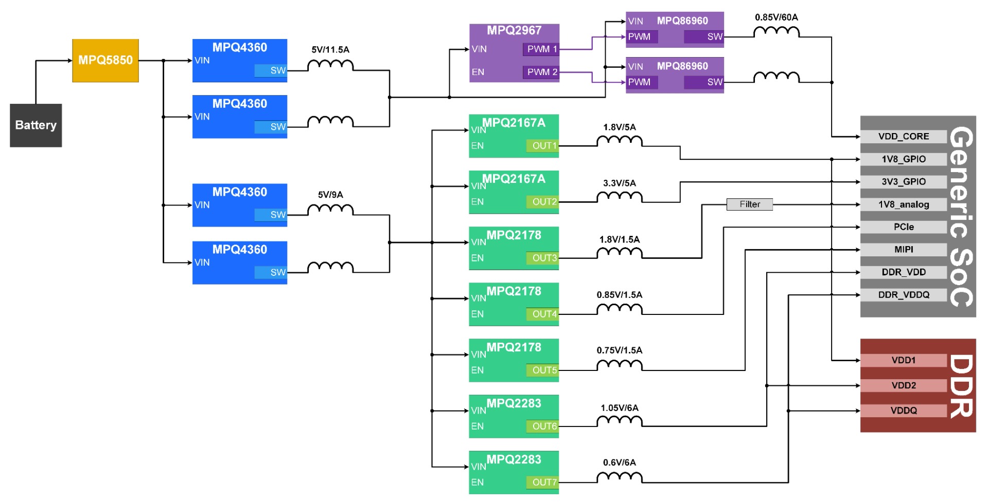
图5: 最终SoC电源树
结语
本文探讨了基于PoL变换器的汽车 SoC 电源树设计,并阐述了如何选择一款兼具性能与成本优势的 IC,文章还对决定汽车应用最佳组件选择的关键因素进行了说明。总而言之,汽车SoC 电源树设计可以概括为两个步骤:第一步确定每条电源轨的关键要求,包括效率、精度、噪声以及成本;第二步确定哪种器件最能满足这些要求。MPS官网提供了便捷的方法供设计师比较并找到适合应用的最佳器件,请访问开关变换器和控制器(车规级),获取更多信息。
_______________________
您感兴趣吗?点击订阅,我们将每月为您发送最具价值的资讯!
技术论坛
 Latest activity 2 years ago
 10 回复
Latest activity 2 years ago
4 回复
Latest activity a year ago
10 回复
10 回复
Latest activity 2 years ago
4 回复
Latest activity a year ago
10 回复
直接登录
创建新帐号