MEZS7-PDCharger-MP2760 参考设计

简介
MEZS7 -PDCharger-MP2760是采用 MP2760 和 MPF52002这两款器件为双角色端口 (DRP) 应用提供的电源解决方案模块。
MP2760是一款具有 4V 至 22V 输入电压 (VIN) 的升降压充电器 IC,适用于1 至 4 节串联电池组应用。在源模式(供电模式)下,它通过 IN 引脚提供5V至21V宽输入电压范围,符合 USB PD 标准。此外,该器件在源模式下还具有高分辨率输出限流功能。
MPF52002是高度集成的 USB PD 控制器,搭载32 位 ARM Cortex- M0微控制器 (MCU),适用于 DRP 端口。它支持 DRP 应用的自动 DRP 切换,符合PD3.1规范。该器件在源模式下支持PD3.1、BC1.2 、Apple 分压器模式、华为FCP/SCP 和QC2.0/3.0。
MEZS7 -PDCharger-MP2760上包含一个 DRP USB Type-C 端口,并支持PD3.1和BC1.2协议。当插入适配器时,该端口作为接收器端口,以最大6A 的充电电流为电池充电;当插入负载时,该端口则作为供电端口,通过电池为USB VBUS 供电。
性能总结 (1)
以下规格参数均基于 TA = 25°C 条件,除非另有说明。
| 参数 | 条件 | 默认值 |
| 接收模式 | ||
| 输入电压(VIN)范围 | 4V 至 22V | |
| 输入电流(IIN)限制 | 高达 5A | |
| 电池充电调节电压 (VBATT_REG) (2) | 8.4V | |
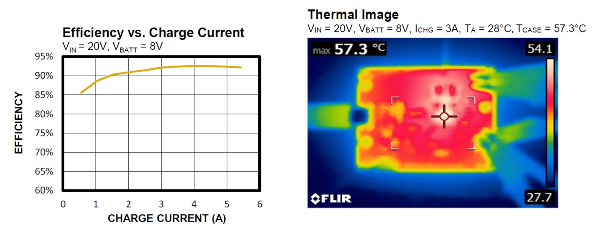
| 快充电流 (2) | VIN = 9V 至 20V | 3A |
| 典型充电效率 | VIN = 20V, VBATT = 8V, ICC = 3A |
92.2% |
| 源模式(供电模式) | ||
| 电池电压范围 | 高达 18.72V | |
| 源模式下的输出电压 (VIN_SRC) (3) | 5V 至 21V | |
| 默认PDO输出 | 5V/3A, 9V/3A, 15V/1.8A, 20V/1.35A, 5V 至 5.9V/3A, 5V 至 11V/3A, 5V 至 16V/1.8A | |
| 源模式典型效率 | VBATT = 8V, VIN_SRC = 9V, IIN_SRC = 2.6A | 93.6% |
1) 更多详细信息请参阅MP2760数据手册;
2) MPF52002可通过 I2C 接口对该参数进行配置;
3) MPF52002根据协议对该参数进行自动配置。
评估板
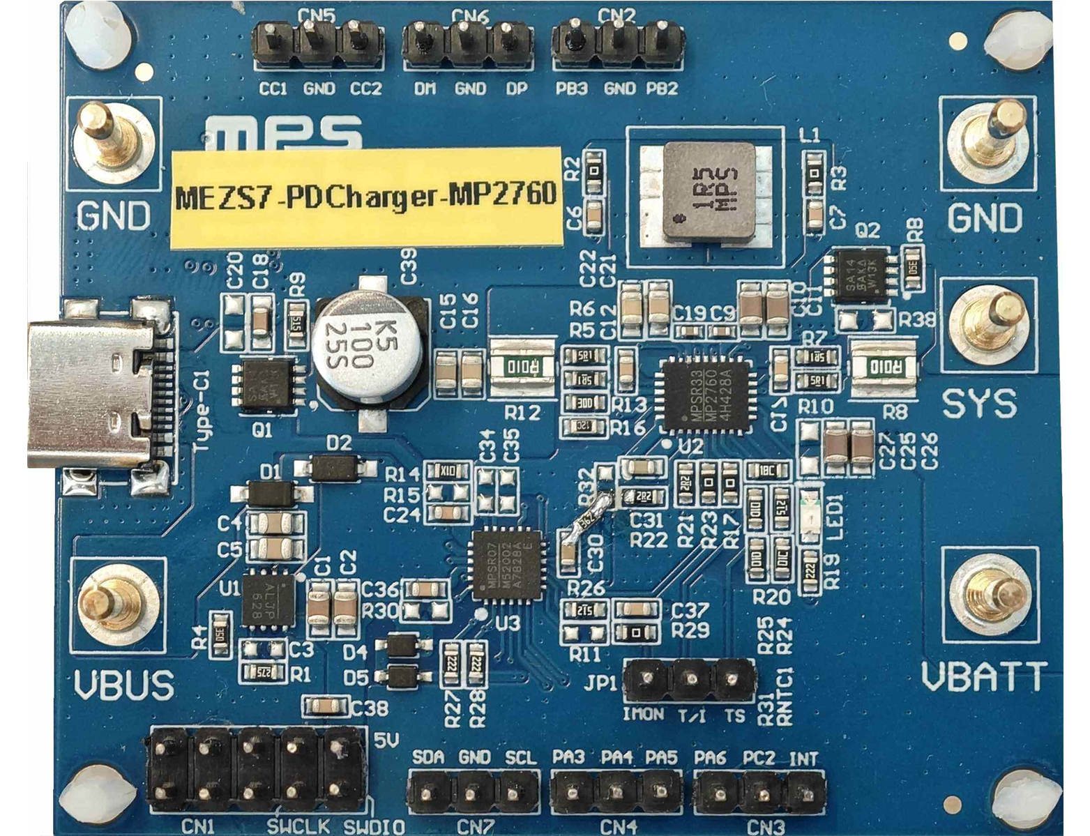
长x宽x高 (6cmx5cmx2.1cm)
| 评估板型号 | MPS IC 型号 |
| MEZS7-PDCharger-MP2760 | MPF52002GRE-001C |
| MP2760GVT-000A |
表 1:电池数量和 VSYS_MIN 设置 (4)
| 电池数量 | VSYS_MIN | PB2 | PB3 |
| 2节(默认) | 6.2V | 1:浮空或高 | 1:浮空或高 |
| 3节 | 9V | 0:短接至GND | 1:浮空或高 |
| 4节 | 12V | 1:浮空或高 | 0:短接至GND |
4) 在对实际电池进行充电之前,先设置PB2和PB3以配置电池数量和 VSYS_MIN。
快速入门指南
MEZS7-PDCharger-MP2760 是采用MP2760和MPF52002这两款器件实现的 2 至 4 节串联电池供电 (PD) 充电器模块。该模块提供了PD 应用参考设计,它包含一个 DRP USB Type-C 端口。如果是2 节串联锂离子电池,充电电流预设为3A ,满电电压预设为8.4V 。在反向供电模式下,输出预设为5V/3A或27W PD。所有充电/放电参数均由MPF52002设置。
用户可以在启动后通过 I2C 接口将自定义的充电参数设置下载到MPF52002 的易失性存储器中;或者下载到MPF52002 的非易失性存储器 ( NVM ) 中,NVM即使在器件完全断电的条件下也不会被重置。
然后,按照以下步骤连接电池和负载以进行测试:
- 将串联电池端子连接至:
- 正极 (+): VBATT
- Negative (-): GND
- 正极 (+): VBATT
- 负极 (-): GND
- 确保电池电压存在(如果采用电池仿真器,请保持其开启)。
- 将系统负载端子连接至:
- 正极 (+): SYS
- 负极 (-): GND
如果采用电池仿真器,则先预设电池电压,然后关闭,再将电池仿真器的输出端子连接到:
在适配器插入之前,确保PB2和PB3正确设置(见表1),以避免损坏系统负载和电池。
接收模式
采用 USB Type-C 转 Type-C 或 Type-A 转 Type-C 数据线,将 USB Type-C 端口与适配器相连。MP2760将根据适配器和电路板之间的自动协商结果设置 IIN_LIM 和适配器输出电压。然后,充电器开始工作。
评估板上的MPF52002默认固件在接收模式下支持以下协议:
- PD3.1
- 对于非 PD 适配器,总线电压 (VBUS) 为5V 。默认输入电流 (IIN) 限值为900mA 。若检测到源端CC引脚配置了Rp电阻,则根据Rp阻值提升 IIN_LIM 至1.5A或3A。
The MPF52002 将根据适配器协议自动请求最大输入功率。
The MPF52002 先向MP2760发送 I2C 命令,然后MP2760对电池进行充电。对于 2 节电池应用,默认最小系统电压 (VSYS_MIN) 为6.2V ,默认电池满电调节电压为8.4V。CC充电电流限制默认设置为3A 。
如果输入功率足够高,则充电电流默认为3A 。如果输入功率不够高,则实际充电电流可能会受输入功率的限制。当适配器最大功率低于最大充电功率额定值时,输入限流环路会调整充电电流,以避免电源/适配器过载。
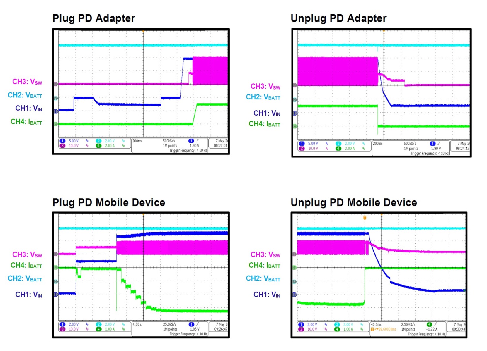
图 1 显示了接收模式设置。
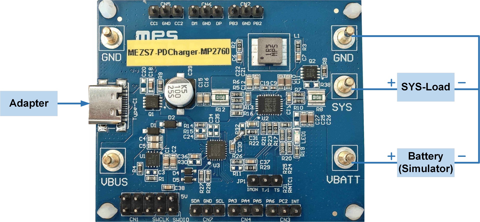
图 1:接收模式设置
源模式
采用USB Type-C 转 Type-C、Type-C 转 micro-B 或 Type-C 转 Lighting 线缆,将器件连接到 USB Type-C 端口。源模式可自动启动,并根据器件需求提供合适的电压。
评估板上的MPF52002默认固件在源模式下支持以下协议:
- PD3.1
- DCP
- Apple 模式
VBUS应以 PD 协议分析仪或移动设备设置的默认电压自动启动。PD 协议分析仪可选择不同的PDO输出。
默认PD输出功率为27W,电池放电限流值为6.4A 。
图 2 显示了源模式设置。
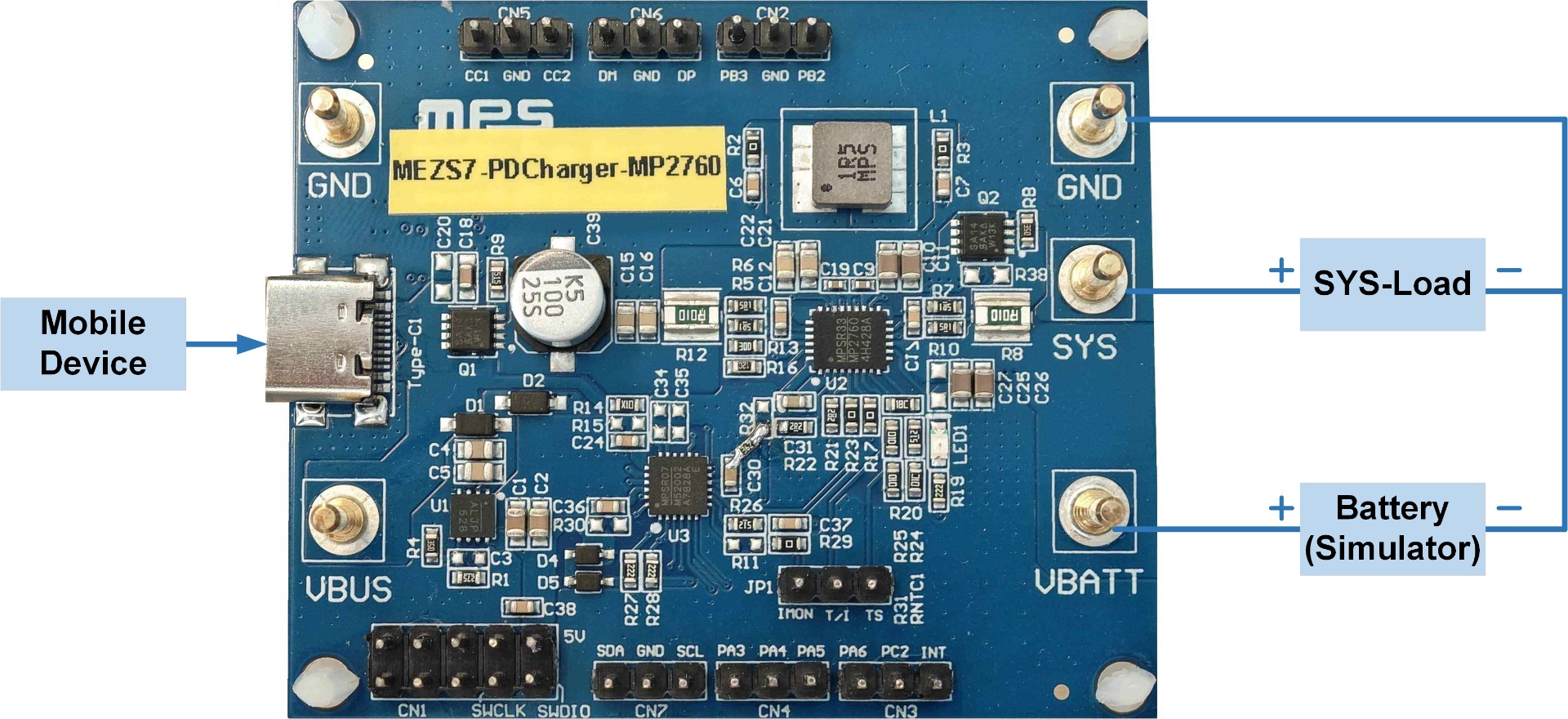
图 2:源模式设置
I2C Target(从设备)功能描述
MP2760 和 MPF52002 可通过 I2C 接口进行控制或监控(见图 3)。主控设备(I2C Initiator)应通过MPF52002的 I2C 接口(PB6和PB7引脚)连接,而非直接连接至MP2760。MPF52002会定期读取MP2760的充电参数和告警状态,并将信息更新至 I2C 从设备寄存器。主控设备也可通过MPF52002向MP2760发送特定的 I2C 指令。
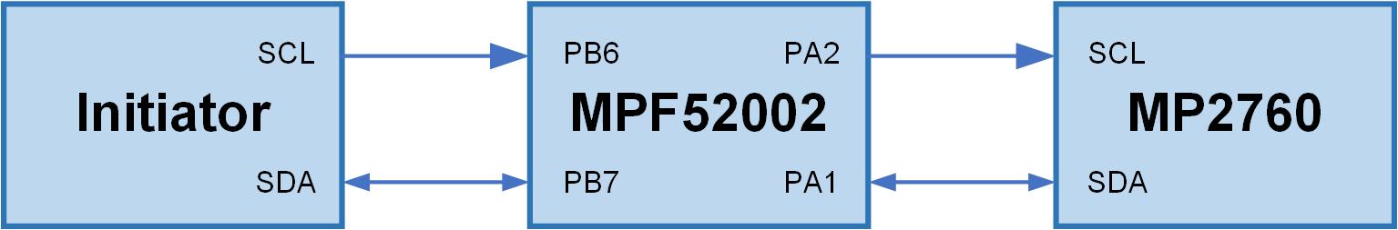
图 3: MPF52002的I2C 从设备功能框图
I2C 连接硬件设置
当设备仅使用电池供电且 I2C 从设备被禁用时,MPF52002 会进入深度睡眠模式以节省电量。通过以下两种方法可以唤醒MPF52002和 I2C 从设备功能,以启动 I2C 通信:
- 在仅电池供电模式下,将PB1 ( CN3中的 INT 引脚)短接至GND 。
- USB Type-C 设备或适配器连接到 USB Type-C 端口。
通信被唤醒后,用接口设备( EVKT-USBI2C-02通信接口)连接PC和评估板。I2C的 SCL应连接到标有SWDIO丝印的PB6引脚;I2C的SDA应连接至标有SWCLK丝印的PB7引脚 (见图 4)。
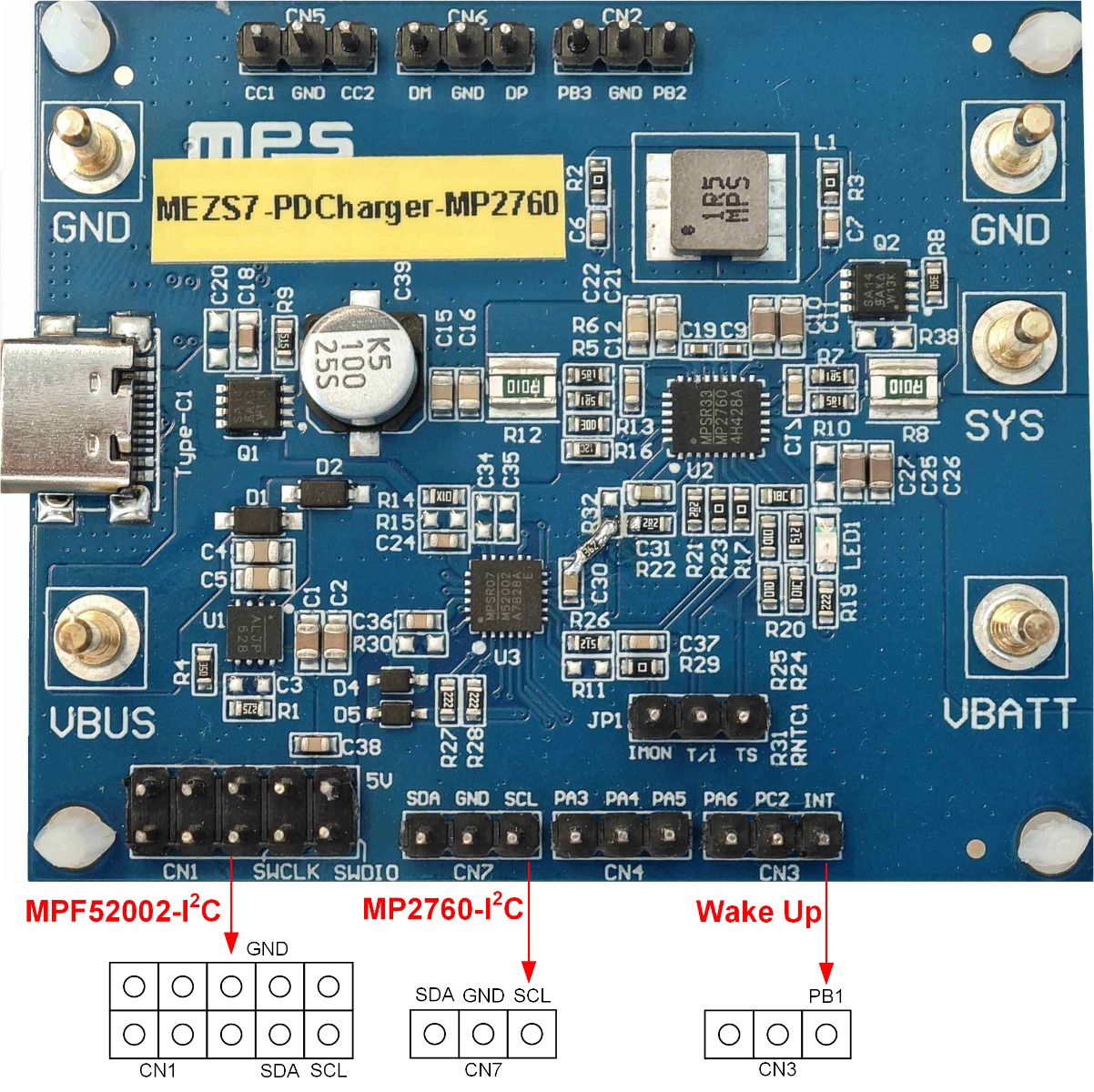
图4:I2C 通信硬件连接
I2C 主控设备的时间要求
- 主控设备的SCL时钟频率为400kHz (快速模式),与100kHz至400kHz时钟频率兼容。
- 每条命令读取或写入 1 个字节,不支持读/写多个字节。
- 建议两个 I2C 命令之间设置10ms (或更长)延迟。
评估板原理图
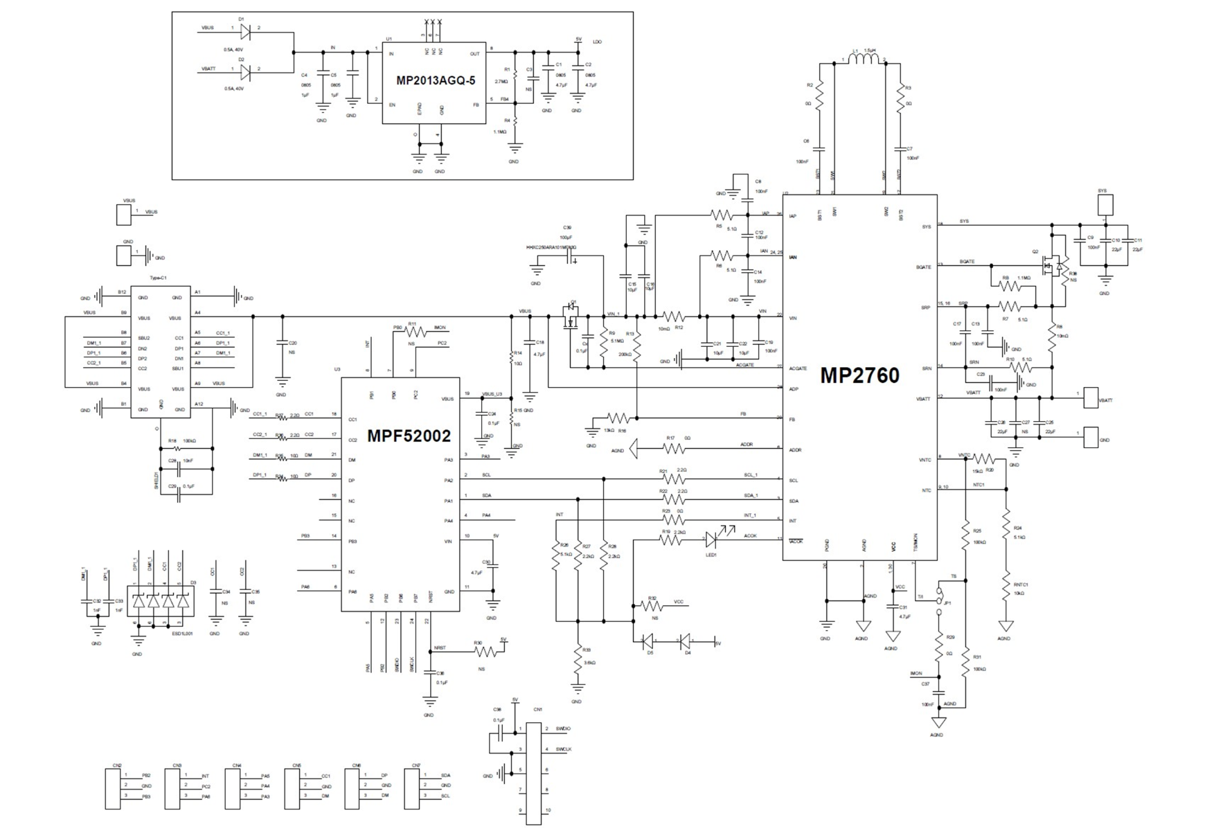
图5:评估板原理图
解决方案模块测试结果
以下性能曲线和波形均在评估板上测得。测试条件:输入电源为PD适配器、VIN = 20V, VBATT = 8V, TA = 25°C、默认寄存器数据,除非另有说明。
直接登录
创建新帐号