AN233 - 采用 BGA/LGA 封装的 MPM 电源模块表面贴装指南

每月为您发送最具参考价值的行业文章
我们会保障您的隐私
摘要
本应用说明对采用 BGA 和 LGA 封装的 MPM 电源模块在组装过程中的关键注意事项进行了全面说明,内容涵盖设计与制造要求,以确保模块在各类电子应用中实现最佳性能、高可靠性以及长期稳定运行。正确的操作、PCB 设计以及返修策略对于降低缺陷并提升组装效率十分关键。
简介
球栅阵列(BGA)和焊盘栅列阵列(LGA)封装因能够支持高密度集成而被广泛应用于现代电子组装中。BGA 封装通过焊球实现连接,而 LGA 封装则依赖焊盘直接接触。确保这些封装采用正确的组装工艺,对于产品的长期可靠性和性能至关重要。本应用说明将详细列举实现可靠组装所需的关键步骤。
封装结构
BGA和LGA封装概述
BGA 封装采用焊球阵列结构来实现机械和电气连接。在回流焊过程中,由于熔融焊球的表面张力,该结构有助于实现自对准。相比之下,LGA 封装没有预置焊球,而是依赖 PCB 上印刷的焊膏(见图 1)。LGA 封装具有以下优势:
- 无需焊球,便于操作(无引脚封装);
- 由于结构中没有焊球,相比采用 BGA 封装的相同产品,其高度更低;
- 灵活性高,单个LGA 电源模块可根据引脚需求设计不同尺寸的焊盘。
这也使LGA 封装对钢网设计和焊膏沉积的变化更加敏感。
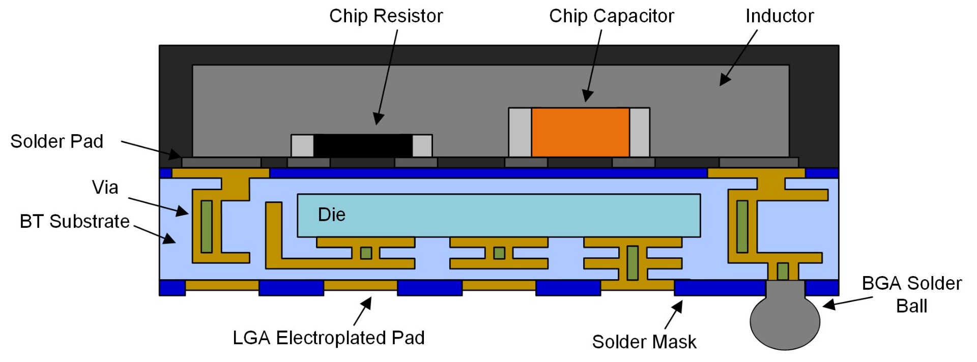
图1:LGA和BGA封装结构
BGA焊盘和焊球形状
BGA 焊盘间距通常在 0.65mm 至 1.27mm 之间,对应的焊盘和焊球尺寸需匹配以确保可靠的连接(见表 1)。
表1: BGA 焊球尺寸
| BGA焊盘间距(P) | 焊盘开窗(A) | 焊球直径(B) | 焊球高度(H) |
|---|---|---|---|
| 0.65 | 0.35 | 0.30 | 0.25 |
| 0.80 | 0.40 | 0.45 | 0.35 |
| 1.00 | 0.45 | 0.50 | 0.37 |
| 1.27 | 0.63 | 0.75 | 0.60 |
对于无铅应用,焊球通常采用 SnAgCu(SAC305);对于传统应用,则采用 SnPb,其尺寸根据不同间距需求进行定制(见图 2)。
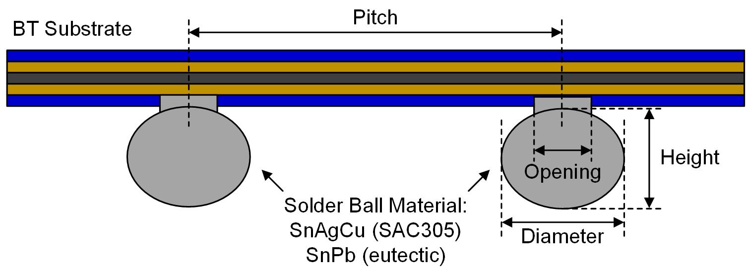
图2: BGA 焊球形状
LGA焊盘表面处理
LGA 焊盘通常采用电镀镍金或化学镀镍钯金(ENEPIG)处理。这些表面处理能够提高可焊性并确保稳定的电气连接。镍层厚度通常为 3µm 至 15µm,金层厚度通常为 0.1µm 至 1.0µm,以确保与焊膏形成可靠连接(见表 2)。
Table 2: LGA 焊盘表面处理尺寸
| 表面处理类型 | 镍(Ni)厚度 | 金(Au)厚度 | 钯(Pd)厚度 |
|---|---|---|---|
| 电镀 | 3µm至15µm | 0.1µm至1.0µm | N/A |
| ENEPIG | 2µm至8µm | 0.05µm至0.15µm | 0.05µm至0.15µm |
PCB设计指南
良好的 PCB 设计对于确保 BGA 和 LGA 封装的电气连接可靠性、可制造性以及长期稳定性能极为重要。在 PCB 布局过程中,需要重点考虑焊盘设计、阻焊定义以及信号完整性等因素。
SMD焊盘设计
阻焊定义焊盘(SMD)设计中,阻焊层部分覆盖在 PCB 焊盘边缘(见图 3)。阻焊开口略小于焊盘尺寸,从而在阻焊层与焊盘层之间形成重叠区域。SMD 焊盘设计具有多个优点,例如,阻焊层的覆盖有助于防止焊盘因热或机械应力从 PCB 表面剥离。但该设计也存在缺点,即重叠区域会形成额外界面,不利于系统级应用中的热机械应力管理。
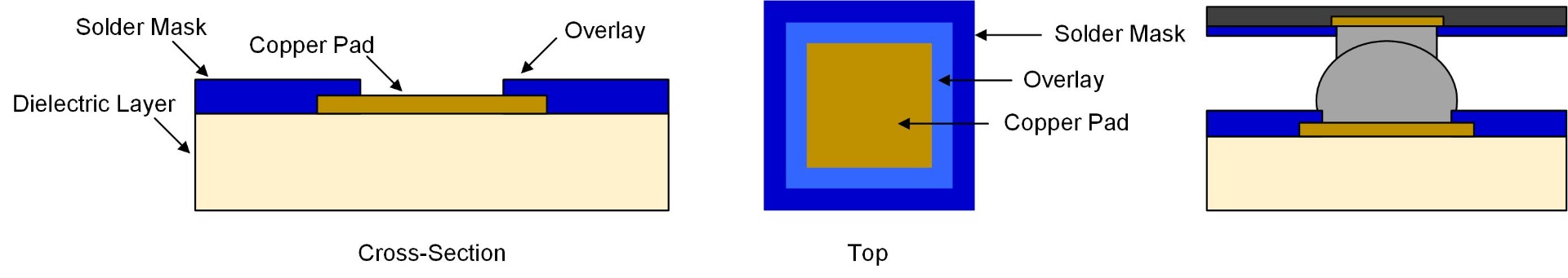
图3:SMD 焊盘示意图
NSMD焊盘设计
对于非阻焊定义焊盘(NSMD),阻焊层与铜焊盘之间存在间隙(见图 4)。在这种结构中,焊膏印刷区域仅由铜焊盘尺寸决定,而非阻焊层。由于焊膏覆盖整个焊盘,NSMD 焊盘通常具有更好的焊接连接和更高的焊点可靠性。但在组装中或特殊工况下,这类焊盘更容易从 PCB 上剥离。
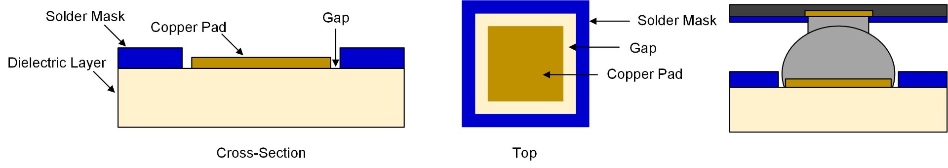
图4: NSMD 焊盘示意图
表3 和 表4 分别给出了 SMD 和 NSMD 焊盘及阻焊开口的尺寸。表3 适用于 BGA 圆形焊盘,表4 适用于 LGA 方形焊盘。
表3:BGA PCB焊盘布局(圆形焊盘)
| 间距 (P) (mm) | SMD焊盘-金属焊盘尺寸(B)(mm) | SMD焊盘-阻焊开窗(A)(mm) | NSMD焊盘-金属焊盘尺寸(B1)(mm) | NSMD焊盘-阻焊开窗(A1)(mm) |
|---|---|---|---|---|
| 0.65 | ≥ 0.45 | 0.35 | 0.35 | ≥ 0.45 |
| 0.80 | ≥ 0.50 | 0.40 | 0.40 | ≥ 0.50 |
| 1.00 | ≥ 0.60 | 0.50 | 0.50 | ≥ 0.60 |
| 1.27 | ≥ 0.73 | 0.63 | 0.63 | ≥ 0.73 |
表4:LGA PCB焊盘布局(方形焊盘)
| 间距(P)(mm) | SMD焊盘-金属焊盘尺寸(B)(mm) | SMD焊盘-阻焊开窗(A)(mm) | NSMD焊盘-金属焊盘尺寸(B1)(mm) | NSMD焊盘-阻焊开窗(A1)(mm) |
|---|---|---|---|---|
| 1.27 | ≥ 0.73 | 0.630 | 0.630 | ≥ 0.73 |
焊盘内过孔设计
为了改善散热和电气性能,通常会在 PCB 铜焊盘下方布置通孔或埋孔,这种设计称为焊盘内过孔(via-in-pad,见图 5)。该设计会对 PCBA 工艺产生影响,例如焊膏印刷。
开放式散热过孔可直接布置在焊盘下方。可以采用以下方法提升焊接性能:
- 在不显著影响电气和热性能的情况下,将过孔移动至阻焊覆盖区域内;
- 使用铜、环氧树脂或其他材料填充过孔(这可能增加 PCB 制造成本)。
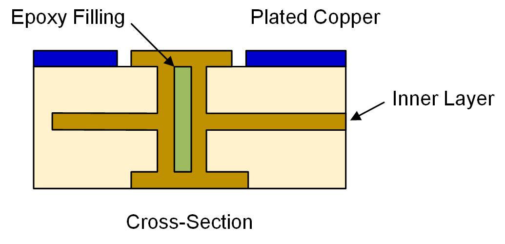
图5: 焊盘内过孔结构示意图
BGA PCB焊盘布局
对于 BGA 封装,通常推荐使用 SMD 焊盘设计,因其能够更好地控制焊点形成。但焊盘尺寸和阻焊开口必须合理定义,以避免焊桥或焊接不足。同时应保持适当的焊盘间距,以确保良好的可焊性并降低短路风险。铜焊盘直径应与焊球尺寸匹配,以在回流过程中实现最佳润湿效果。
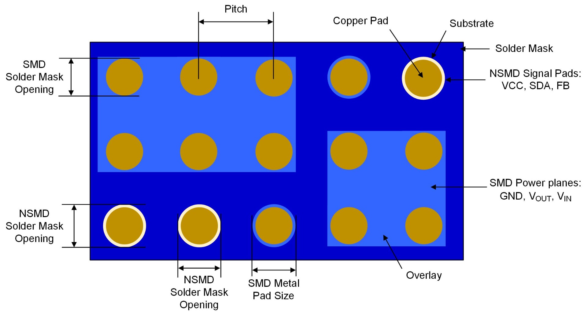
图6: BGA 焊盘推荐设计
LGA PCB焊盘布局
对于采用LGA 封装的 MPS 电源模块,通常推荐采用混合焊盘设计以提高可靠性,尤其是在大电流应用中。
由于信号引脚传输功率较小,其承受的热应力和机械应力较低,因此通常采用 NSMD 焊盘设计,以获得更好的焊接连接和焊点可靠性。
相比之下,功率焊盘需要较大的铜面积,尤其是在高功率模块中。同时功率焊盘承受较大的热和机械应力,因此推荐采用 SMD 焊盘设计。
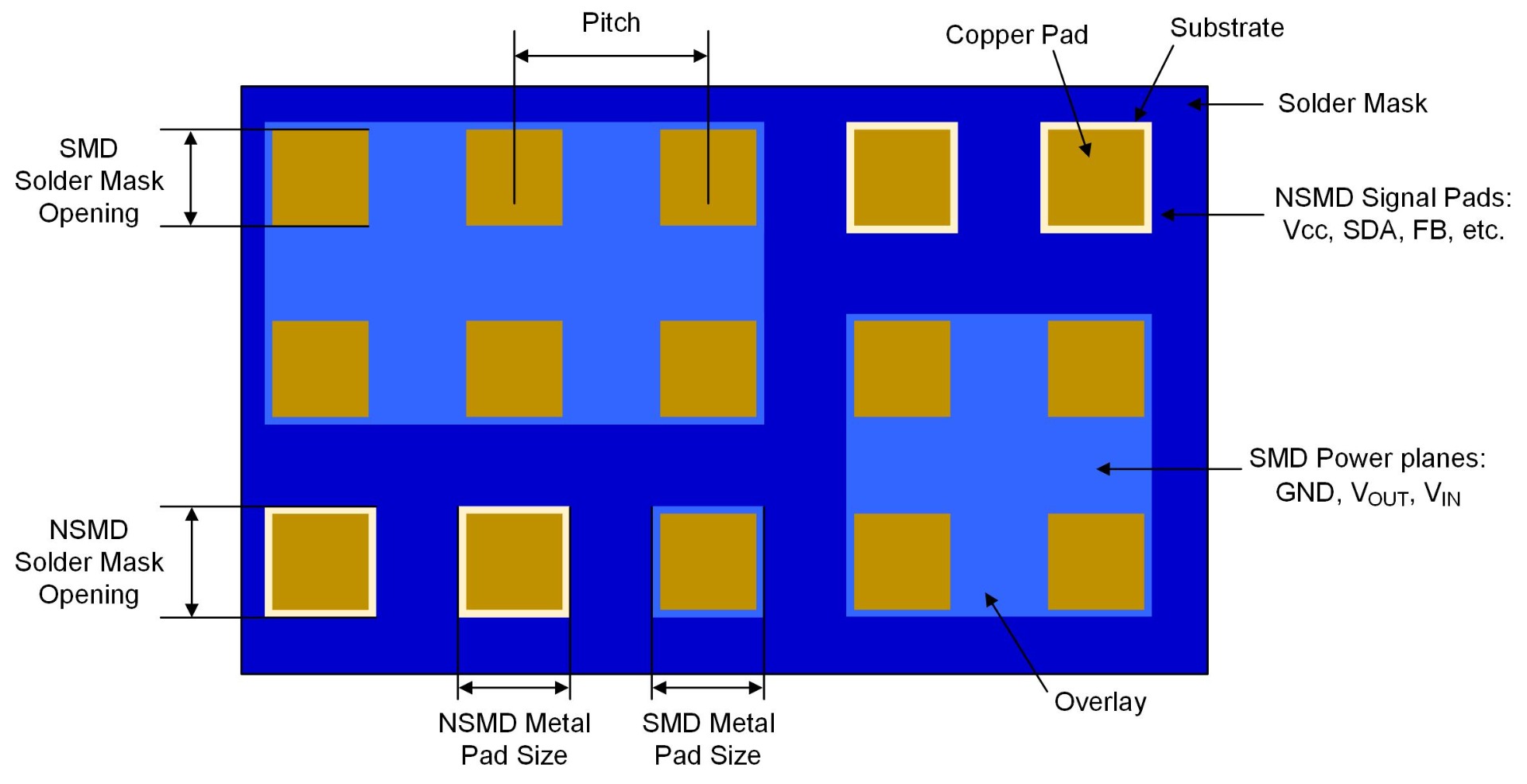
图7: LGA 焊盘推荐设计
图8 展示了采用混合焊盘设计的 PCB 设计示例。该设计基于MPM54304,其封装为 LGA-33(7mm×7mm×2mm)。所有功率焊盘(包括中间的大面积 GND 焊盘)均采用 SMD 设计,而所有信号焊盘(包括 FB、SDA 和 SCL)均采用 NSMD 设计。
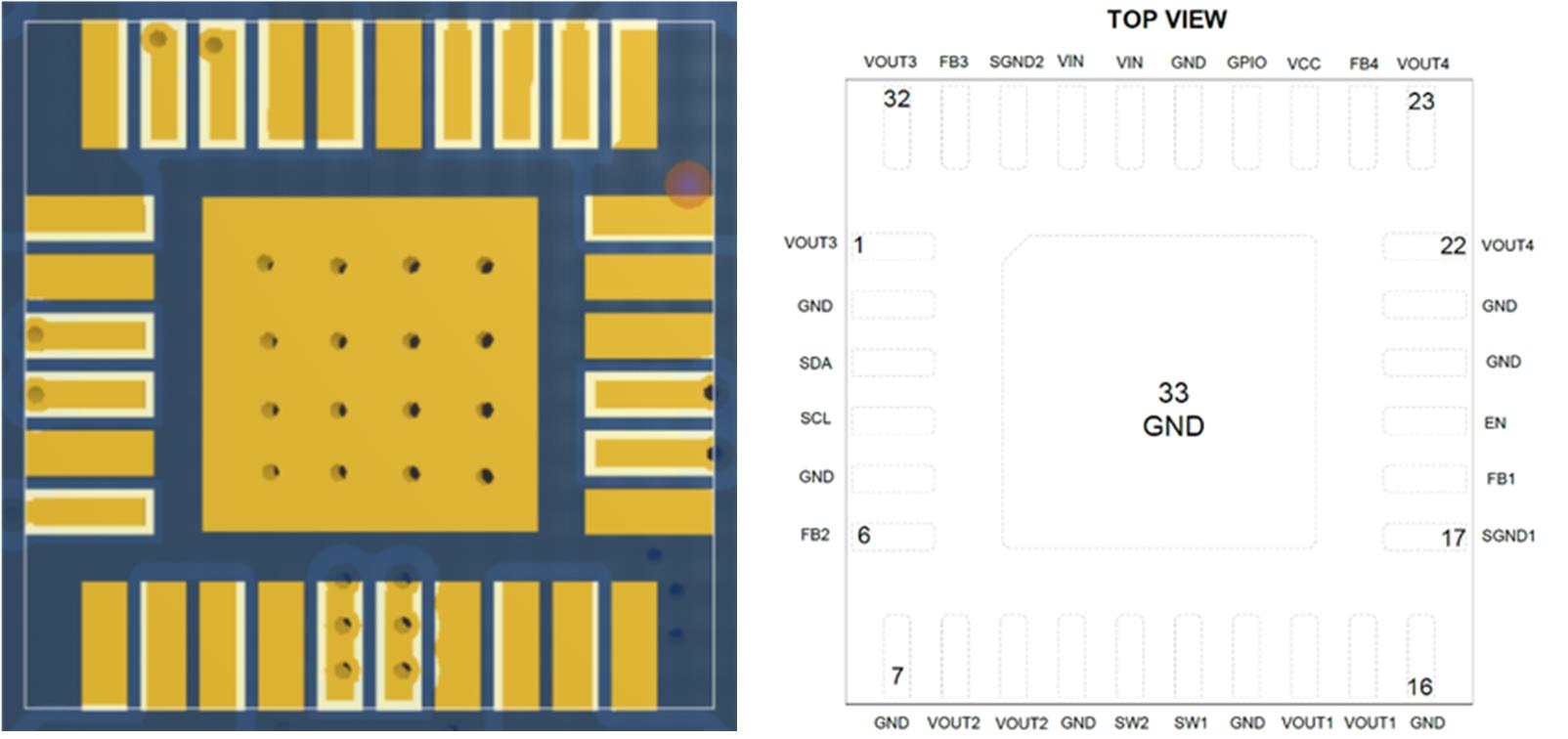
图8: MPM54304封装焊盘示例
PCB 平面分割与隔离焊盘设计
为保证信号完整性并避免不必要的电气干扰,应合理进行 PCB 平面分割设计(见图 9)。在高频应用中,需要进行受控阻抗布线,同时应合理布置电源层和地层,以降低噪声和干扰。
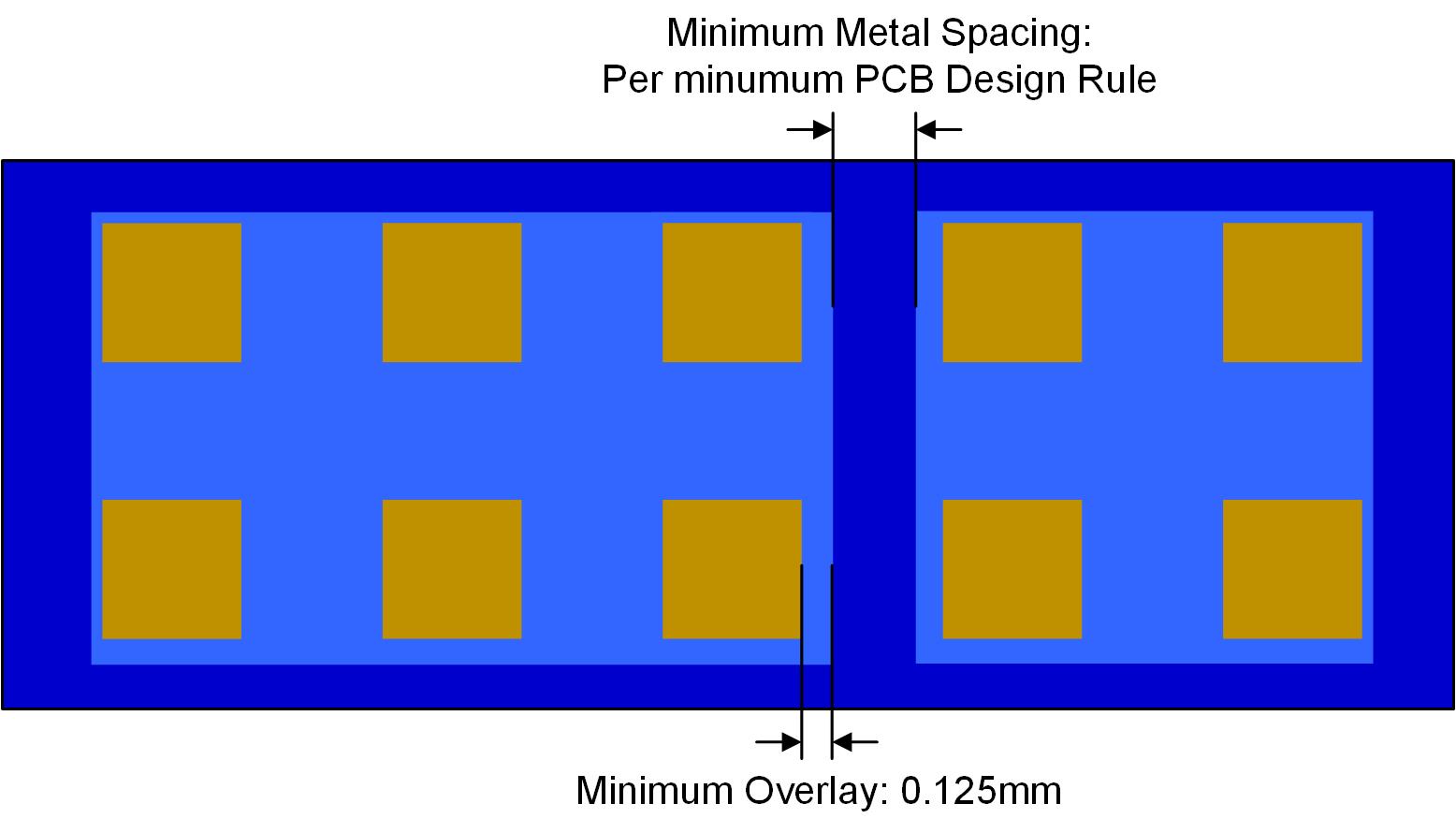
图 9: 平面分割建议
过孔布局与布线考量
对于 BGA 和 LGA 封装,过孔布局对于维持信号完整性和制造可行性至关重要。过孔不应过于靠近焊盘边缘,否则可能导致焊料流失并形成薄弱焊点。在高密度应用中,可以采用焊盘内过孔技术,但需要进行填孔和封孔处理以避免焊接空洞。布线亦应优化,以缩短走线长度并减少阻抗不连续,从而确保稳定的电气性能(见图 10)。
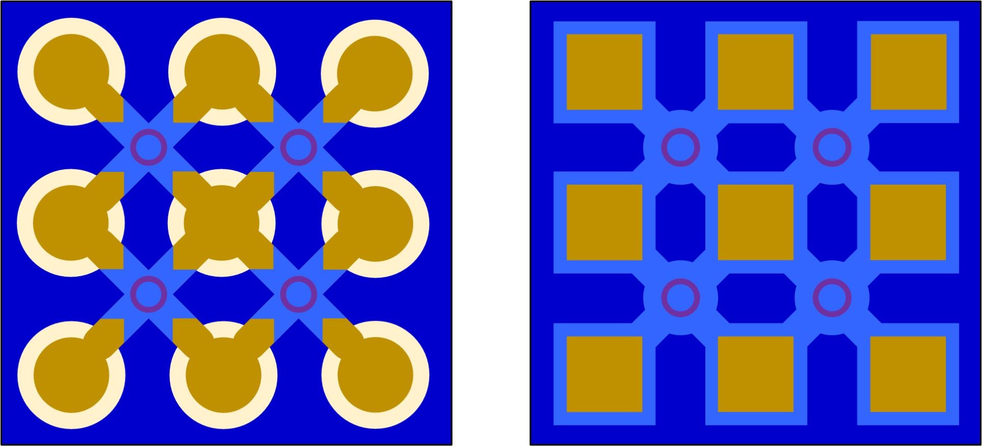
图 10: LGA 和 BGA 热释放过孔布局建议
焊膏涂覆注意事项
精确的焊膏印刷对BGA 和 LGA 封装也很关键。不均匀的焊膏沉积可能导致开路或产生过多空洞。应合理选择钢网厚度、开口尺寸以及焊膏类型,以实现均匀且可靠的焊点。对于超细间距器件,可能需要采用阶梯钢网或电铸钢网以精确控制焊膏体积。
湿度敏感性考量
所有塑封 IC 器件都会吸收水分。在表面贴装过程中,回流焊加热会使水分汽化,从而在封装内部产生应力,继而导致塑封材料开裂。这一现象通常称为“爆米花效应”。
塑封开裂可能导致内部损伤,或使污染物渗入至芯片,从而降低半导体器件的可靠性。
由于塑封器件的吸湿性,在回流焊之前应避免其长时间暴露于相对湿度(RH)超过 10% 的环境中。如果暴露导致吸收了过多水分,则应在回流焊之前进行烘烤以去除水分。
所有 MPS 表面贴装 IC 均具有湿敏等级(MSL)和峰值回流等级标识,该信息标注在卷盘、防潮袋(MBB)以及外包装箱上。MPS 电源模块符合 IPC/JEDEC J-STD-020 标准,MSL 等级为 3 或 4。图11 展示了 MPS 出货标签示例。
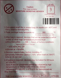
图11: 湿敏等级标签示例
干燥包装要求
表 5 显示了不同湿敏等级的干燥包装要求。
表5: 干燥包装要求
| MSL 等级 | 封袋前干燥 | 带湿度指示卡(HIC)的防潮袋(MBB) | 干燥剂 | MSID 标签 | 警示标签 |
|---|---|---|---|---|---|
| 1 | 可选 | 可选 | 可选 | 非必需 | 若回流温度为 220°C 至 225°C,则不需要;否则需要 |
| 2 | 可选 | 必需 | 必需 | 必需 | 必需 |
| 2a-5a | 必需 | 必需 | 必需 | 必需 | 必需 |
| 6 | 可选 | 可选 | 可选 | 必需 | 必需 |
车间寿命
SMD 器件的车间寿命(floor life)会受到非 30°C/60% RH 环境条件的影响(见表 6)。
表6: 湿敏等级与车间寿命
| MSL 等级 | 在 ≤30°C/60% RH 条件下的车间寿命(拆袋后) |
|---|---|
| 1 | 无限制 |
| 2 | 1 年 |
| 2a | 4 周 |
| 3 | 168 小时 |
| 4 | 72小时 |
| 5 | 48小时 |
| 5a | 24小时 |
| 6 | 使用前必须烘烤,烘烤后必须在标签规定时间内完成回流 |
SMD器件的干燥处理
对于 MSL 等级为 2 至 5a 且已超过车间寿命的器件,可按照表 7(回流前再烘烤)或表 8(干燥包装前烘烤)进行干燥处理。
表7: 贴装或非贴装 SMD 封装的干燥参考条件(用户烘烤:烘烤完成后,车间寿命计时从 Time =0开始)(1)
| 封装体(3) | MSL等级 | 烘烤温度 125°C (+10/-0°C),相对湿度 <5% | 烘烤温度 90°C (+8/-0°C),相对湿度 ≤5% | 烘烤温度 40°C (+5/-0°C),相对湿度 ≤5% | |||
|---|---|---|---|---|---|---|---|
| 超出车间寿命 >72h | 超出车间寿命 <72h | 超出车间寿命 >72h | 超出车间寿命 <72h | 超出车间寿命 >72h | 超出车间寿命 <72h | ||
| 厚度 ≤0.5 mm(5) | 2 | 无需(4) | 无需(4) | 无需(4) | 无需(4) | 无需(4) | 无需(4) |
| 2a | 1小时 | 1小时 | 2小时 | 1小时 | 12小时 | 8小时 | |
| 3 | 1小时 | 1小时 | 3小时 | 1小时 | 22小时 | 8小时 | |
| 4 | 1小时 | 1小时 | 3小时 | 1小时 | 22小时 | 8小时 | |
| 5 | 1小时 | 1小时 | 3小时 | 1小时 | 23小时 | 8小时 | |
| 5a | 1小时 | 1小时 | 4小时 | 1小时 | 26小时 | 8小时 | |
| 厚度 >0.5 mm, ≤0.8 mm(5) | 2 | 无需(4) | 无需(4) | 无需(4) | 无需(4) | 无需(4) | 无需(4) |
| 2a | 4小时 | 3小时 | 15小时 | 13小时 | 4天 | 3天 | |
| 3 | 4小时 | 3小时 | 15小时 | 13小时 | 4天 | 3天 | |
| 4 | 4小时 | 3小时 | 16小时 | 13小时 | 4天 | 3天 | |
| 5 | 4小时 | 3小时 | 16小时 | 13小时 | 4天 | 3天 | |
| 5a | 4小时 | 3小时 | 16小时 | 13小时 | 4天 | 3天 | |
| 厚度 >0.8 mm, ≤1.4 mm(5) | 2 | 无需(4) | 无需(4) | 无需(4) | 无需(4) | 无需(4) | 无需(4) |
| 2a | 8 hours | 6小时 | 25 hours | 20小时 | 8 days | 7天 | |
| 3 | 8 hours | 6小时 | 25 hours | 20小时 | 8 days | 7天 | |
| 4 | 9小时 | 6小时 | 27小时 | 20小时 | 10天 | 7天 | |
| 5 | 10小时 | 6小时 | 28小时 | 20小时 | 11天 | 7天 | |
| 5a | 11小时 | 6小时 | 30小时 | 20小时 | 12天 | 7天 | |
| 厚度 >1.4 mm, ≤2.0 mm | 2 | 18小时 | 15小时 | 63小时 | 2 days | 25天 | 20天 |
| 2a | 21小时 | 16小时 | 3天 | 2天 | 29天 | 22天 | |
| 3 | 27小时 | 17小时 | 4天 | 2天 | 37天 | 23天 | |
| 4 | 34小时 | 20小时 | 5天 | 3天 | 47天 | 28天 | |
| 5 | 40小时 | 25小时 | 6天 | 4天 | 57天 | 35天 | |
| 5a | 48小时 | 40小时 | 8天 | 6天 | 79天 | 56天 | |
| 厚度 >2.0 mm, ≤4.5 mm | 2 | 48小时 | 48小时 | 10天 | 7天 | 79天 | 67天 |
| 2a | 48小时 | 48小时 | 10天 | 7天 | 79天 | 67天 | |
| 3 | 48小时 | 48小时 | 10天 | 8天 | 79天 | 67天 | |
| 4 | 48小时 | 48小时 | 10天 | 10天 | 79天 | 67天 | |
| 5 | 48小时 | 48小时 | 10天 | 10天 | 79天 | 67天 | |
| 5a | 48小时 | 48小时 | >10天 | 10天 | 79天 | 67天 | |
| 针对尺寸 > 17 mm × 17 mm 的 BGA 封装或任何叠芯封装的例外情况 | 2-5a | 96 小时 (2) (5) | 同上(视包装厚度及含水量而定) | 不适用 | 同上(视包装厚度及含水量而定) | 不适用 | 同上(视包装厚度及含水量而定) |
注:
1)表 7 和表 8 基于最坏情况的塑封引线框架 SMD 封装。在大多数情况下,这些数据也适用于其他非气密封装的表面贴装器件。若有技术依据(如吸湿/脱湿数据),可适当缩短烘烤时间。若器件暴露在 >60% RH 环境中,可能需要随时监测脱附数据,延长烘烤时间,以确保部件完全干燥。
2)对于尺寸 >17mm×17mm 且无阻碍水分扩散路径的 BGA 封装,可依据厚度与湿敏等级对应时间进行烘烤。
3)厚度 >4.5mm 的封装请参考 IPC/JEDEC J-STD-033 附录 B。
4) 对于薄型(<1.4 mm)MSL2 器件,若其车间寿命限制在 <30°C 且 <60% RH 的条件下,则无需进行烘烤处理。这是由于此类薄型器件具有特定的水分扩散特性:在 MSL2 级(85°C/60% RH 环境下暴露 168 小时)的吸湿测试完成后,其内部水分已达到完全饱和状态。
5)对于不含阻挡层或堆叠芯片的封装而言,所规定的烘烤时间属于保守设定。对于含有阻碍水分扩散的内部层的堆叠芯片或 BGA 封装,其实际烘烤时间可能长于表 7 中所要求的时长。
表8所示为默认烘烤时间。
表 8:干燥包装前所采用的默认烘烤时间(暴露于 ≤60% RH 条件下)(MET = 24h) (1) (6)
| 封装体厚度 | 等级 | 在 125°C (+10/-0°C) 下烘烤 | 在 150°C (+10/-0°C) 下烘烤 |
|---|---|---|---|
| ≤1.4mm | 2 | 7小时 | 3小时 |
| 2a | 8小时 | 4小时 | |
| 3 | 16小时 | 8小时 | |
| 4 | 21小时 | 10小时 | |
| 5 | 24小时 | 12小时 | |
| 5a | 28小时 | 14小时 | |
| >1.4mm, ≤2.0mm | 2 | 18小时 | 9小时 |
| 2a | 23小时 | 11小时 | |
| 3 | 43小时 | 21小时 | |
| 4 | 48小时 | 24小时 | |
| 5 | 48小时 | 24小时 | |
| 5a | 48小时 | 24小时 | |
| >2.0mm, ≤4.5mm | 2 | 48小时 | 24小时 |
| 2a | 48小时 | 24小时 | |
| 3 | 48小时 | 24小时 | |
| 4 | 48小时 | 24小时 | |
| 5 | 48小时 | 24小时 | |
| 5a | 48小时 | 24小时 |
注:
6) 若需对厚度大于 4.5 mm 的封装进行烘烤,请参阅 IPC/JEDEC J-SDT-033 附录 B。
表 9 显示了如何在重置或暂停车间寿命计时。
表 9: 在用户现场重置或暂停车间寿命
| MSL等级 | 温/湿度暴露时间 | 车间寿命 | 干燥器存放时间(相对湿度) | 烘烤 | 重置货架期(shelf life) |
|---|---|---|---|---|---|
| 2, 2a, 3,4, 5, 5a | 任意时间,≤40°C/85% RH | 重置 | N/A | 参见表 7 | 烘烤后干燥包装 |
| 2, 2a, 3, 4, 5, 5a | > 车间寿命,≤30°C/60% RH | 重置 | N/A | 参见表 7 | 烘烤后干燥包装 |
| 2, 2a, 3 | > 12小时,≤30°C/60% RH | 重置 | N/A | 参见表 7 | 烘烤后干燥包装 |
| 2, 2a, 3 | ≤ 12小时,≤30°C/60% RH | 重置 | 暴露时间的 5 倍(≤10% RH) | N/A | N/A |
| 2, 2a, 3 | 累计时间 < 车间寿命,≤30°C/60% RH | 暂停 | 随时(≤10% RH) | N/A | N/A |
| 4, 5, 5a | > 8小时,≤30°C/60% RH | 重置 | N/A | 参见表 7 | 烘烤后干燥包装 |
| 4, 5, 5a | ≤ 8小时,≤30°C/60% RH | 重置 | 暴露时间的 10 倍(≤5% RH) | N/A | N/A |
货架期(Shelf Life)
在封装密封完好且储存条件低于 40°C/90% RH 的前提下,MPS 模拟 IC 产品的货架期为生产日期起 5 年。
其他保修条款请参考 MPS International Ltd. 标准条款。
板级组装工艺
钢网设计
钢网设计对基于 LGA 封装的 MPS 电源模块组装过程十分重要,因为它决定了每个 LGA 焊盘上焊膏的厚度和体积。在钢网设计过程中必须综合考虑各种工艺和关键参数。在焊膏转移过程中,应优先采用具有高质量开口的先进钢网。
最常见的钢网厚度建议为 4mil 至 5.6mil,钢网开口必须符合各封装规格。对于较大的焊盘(>1mm2),应采用多开口设计,以便更好地分布焊膏。表 10 给出了 BGA 封装的推荐钢网尺寸。表 11 给出了采用方形焊盘的 LGA 封装推荐钢网尺寸。表 12 给出了采用圆形焊盘的 LGA 封装推荐钢网尺寸。
表 10:推荐钢网尺寸(BGA)
| BGA 焊盘间距 (mm) | 焊盘开口(mm) | 钢网开口(mm) | 钢网厚度 (mils) |
|---|---|---|---|
| 0.65 | 0.35 | 0.33 | 4 |
| 0.80 | 0.40 | 0.38 | 4 |
| 1.00 | 0.50 | 0.48 | 4 |
| 1.27 | 0.63 | 0.60 | 4 |
表 11:推荐钢网尺寸(LGA - 方形焊盘)
| LGA 焊盘间距 (mm) | 焊盘开口 (mm) | 钢网开口 (mm) | 钢网厚度 (mils) |
|---|---|---|---|
| 1.27 | 0.63 | 0.60 | 5 |
| 1.27 | 0.89 | 0.84 | 5 |
| 1.27 | 0.76 | 0.72 | 5 |
表 12:推荐钢网尺寸(LGA -圆形焊盘)
| LGA 焊盘间距 (mm) | 焊盘开口 (mm) | 钢网开口 (mm) | 钢网厚度 (mils) |
|---|---|---|---|
| 0.65 | 0.35 | 0.33 | 4 |
| 0.80 | 0.40 | 0.38 | 4 |
| 1.00 | 0.50 | 0.48 | 5 |
| 1.27 | 0.63 | 0.60 | 5 |
PCB 表面处理
PCB 制造中通常可根据应用需求提供多种表面处理方式,包括:
- 有机可焊性保护层(OSP)
- 化学镀镍浸金(ENIG)
- 电镀镍金
- 沉银
- 沉锡
设计工程师、客户或终端用户可根据系统需求选择合适的表面处理方式。MPS 推荐使用 OSP、ENIG 和沉锡以获得最佳效果。每种 PCB 表面处理方式均需根据焊点可靠性及制造工艺进行评估。
焊膏
建议使用 SAC305 焊膏,以符合电子产品无铅法规及 RoHS/REACH 环保要求。对于采用 LGA 封装的 MPS 电源模块,推荐使用 IV 型免清洗焊膏。
印刷工艺
在印刷过程中,焊膏从钢网转移至 PCB 的效率受多种因素影响,包括但不限于刮刀速度、压力和角度(见图 12)。MPS 建议始终遵循焊膏供应商的相关参数建议。
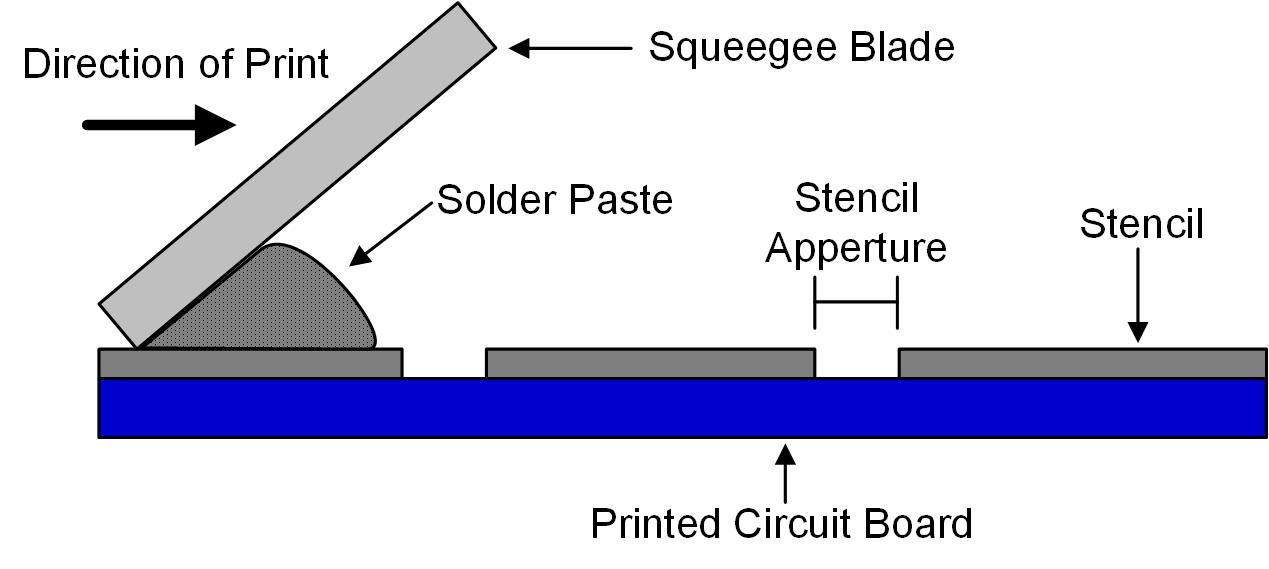
图 12:印刷设备示意图
器件贴装
LGA 器件的贴装也是组装质量的关键环节。建议使用带视觉系统的自动贴片设备。贴装精度应控制在最大 ±30μm。
回流曲线
回流曲线是确保焊点强度并防止空洞、立碑或虚焊等缺陷的关键因素。必须严格遵循推荐的回流曲线,以获得一致的结果。
LGA 器件的回流焊没有特殊要求,但在没有其他说明的情况下,应遵循 JEDEC 标准回流曲线。JEDEC 回流曲线定义了 SMT 组装过程中各加热阶段,每个阶段均规定了温度和时间范围,用于优化特定 PCB 组装的温度曲线。需要注意的是,每个组装设计都是定制的,需要针对整板优化专属回流曲线。详细信息请参考 IPC/JEDEC J-STD-020D 标准。
实际回流参数还取决于所使用的焊膏,请遵循焊膏厂商的建议。
建议使用干燥空气作为回流气氛,也可以使用氮气。同时建议监控封装顶部温度曲线,确保峰值温度不超过器件的 MSL 限值。
建议使用 8 温区或以上并具备氧含量控制的回流炉。MPS 电源模块最多允许回流 3 次。所有 MPS 电源模块均按照无铅峰值回流温度设计。
图13 显示了典型推荐回流曲线。该曲线包含多个温区,每个温区都对焊接质量产生重大影响。
温区划分
典型回流过程包括以下四个阶段:
- 预热区:逐步升温,以避免热冲击
- 恒温区:保持稳定温度以激活助焊剂并均匀加热
- 回流区:达到峰值温度使焊料熔化,形成可靠焊点
- 冷却区:逐步降温,使焊点固化
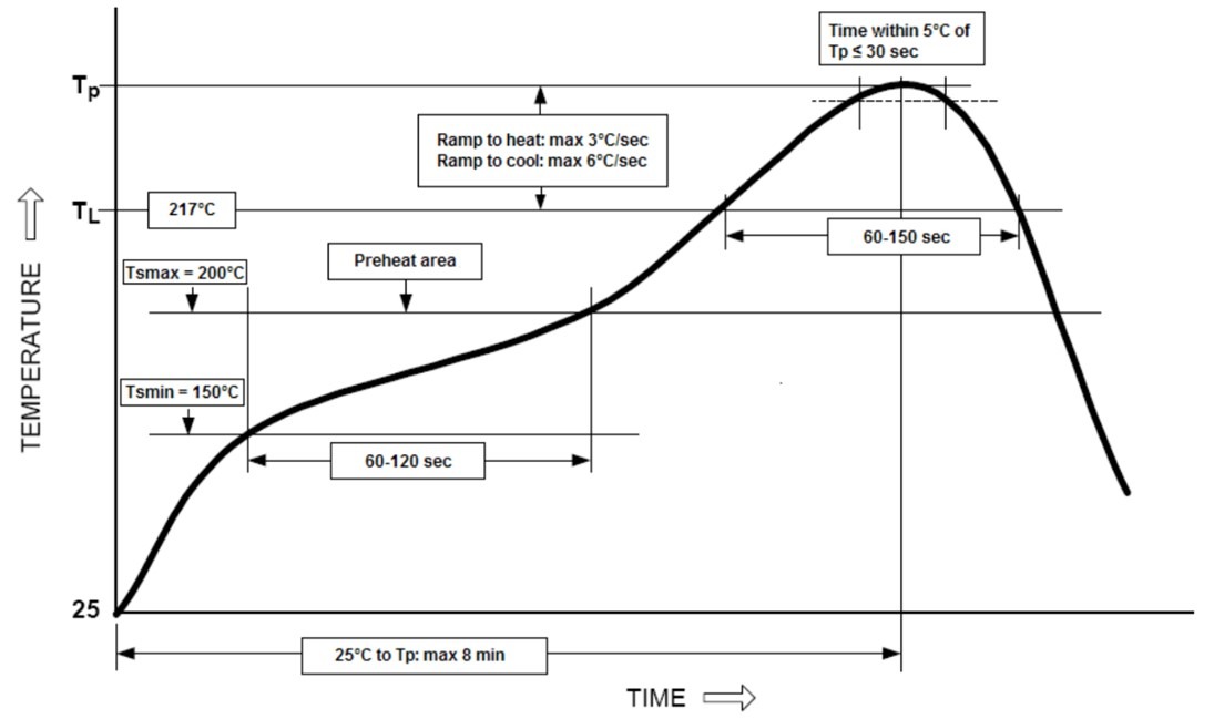
图 13:温度曲线示例
表13 显示了典型回流曲线参数。推荐曲线及参数符合 IPC/JEDEC J-STD-020 标准。
表 13:无铅工艺 - 封装峰值回流温度
| 封装厚度 | 体积 <350mm3 | 体积:350mm3 至 2000mm3 | 体积 ≥ 2000mm3 |
|---|---|---|---|
| < 1.6mm | 260 +0/-5°C | 260 +0/-5°C | 260 +0/-5°C |
| 1.6mm to 2.5mm | 260 +0/-5°C | 250 +0/-5°C | 245 +0/-5°C |
| ≥ 2.5mm | 250 +0/-5°C | 245 +0/-5°C | 245 +0/-5°C |
表 14:回流曲线参数
| 参数项 | 无铅焊料 | 有铅焊料 | |
|---|---|---|---|
| 预热 | 最小恒温温度 (TSMIN) | 150°C | 100°C |
| 最大恒温温度 (TSMAX) | 200°C | 150°C | |
| 恒温时间 (tS) | 60秒至120秒 | 60秒至120秒 | |
| 回流 | 液相线温度 (TL) | 217°C | 183°C |
| 液相以上时间 (t) | 30秒至90秒c | 30秒至90秒 | |
| 封装峰值温度 (TP) | 参见表13 | 参见表13 | |
| 峰值温度±5°C时间 (tP) | 最大30秒 | 最大30秒 | |
| 升温速率 (TSMAX to TP) | 最大2.5°C/秒 | 最大2.5°C/秒 | |
| 降温速率 | 最大2.5°C/秒(建议更低) | 最大2.5°C/秒(建议更低) | |
| 25°C 至峰值时间 | 最大8分钟 | 最大8分钟 | |
清洗
由于 LGA 封装的 MPS 电源模块通常使用免清洗焊膏,因此无需进行清洗。
如果使用水溶性焊膏,建议使用皂化剂和/或去离子水喷淋系统进行清洗,清洗后需确保 PCB 完全干燥。
请遵循焊膏供应商提供的清洗指南。
焊点空洞
尽量减少焊点空洞对保证电气和散热性能也至关重要。目前尚无针对底部端子器件的空洞标准。MPS 建议:信号焊盘空洞最大为 25%,大面积/散热焊盘空洞最大为 50%。
焊膏厂商推荐的回流曲线通常可优化助焊剂活性并减少空洞。但若仍出现较多空洞,则可采用相应优化策略。
空洞减少策略
减少焊点空洞的最佳方式包括:
- 使用低空洞焊膏
- 调整回流恒温时间以改善排气
- 必要时采用真空回流
- 优化钢网设计以控制焊膏量
- 将大焊盘分割为 0.5mm × 0.5mm 小焊盘以利于排气
钢网设计对空洞的影响
焊点空洞来源于焊膏熔融过程中的气体释放。当助焊剂气化形成气泡且无法逸出时,就会形成空洞。该现象与焊膏用量直接相关,因此大焊盘更容易产生空洞。图 14 展示了 MPM3695-25 的钢网设计,其中功率焊盘为单一大开口;图中同时展示了对应的 X射线图像,可观察到明显的大空洞。
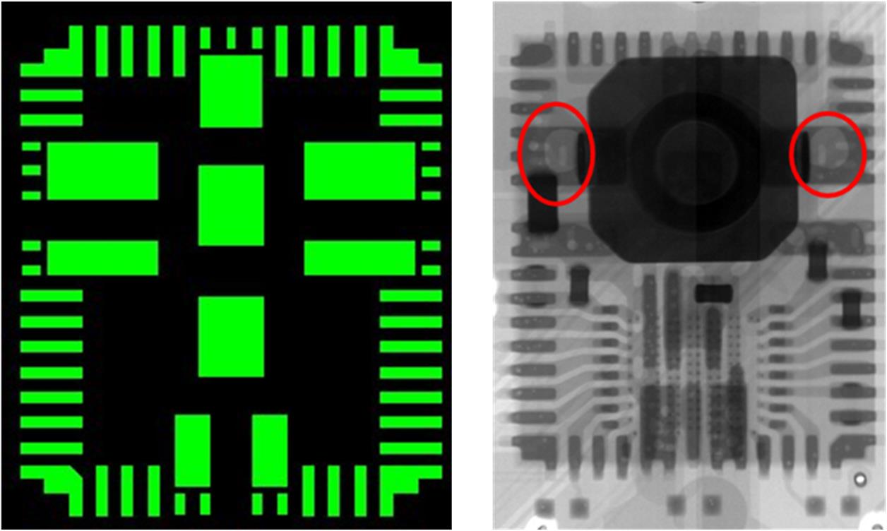
图 14:单开口钢网及 X射线图
将大焊盘分割为多个小开口的钢网设计后,空洞显著减小(见图 15)。
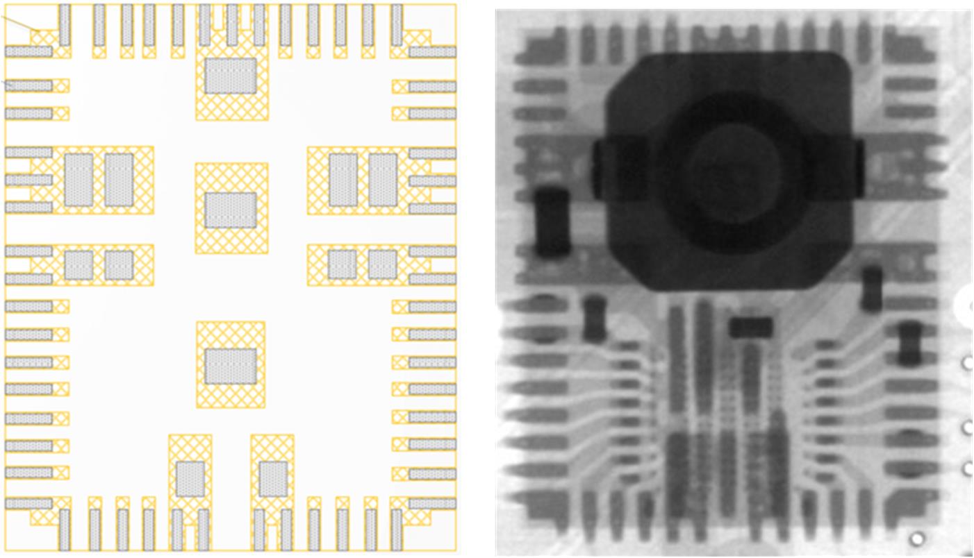
图 15:多开口钢网及 X射线图
双面组装
对于双面 PCB 组装,应评估器件重量与焊盘面积的关系。器件重量/焊盘总面积是否 ≤0.0465gr/mm2,可作为是否适合二次回流的参考。
对于某些 MPS 器件,不建议进行二次回流,包括隔离电源模块、带外露散热器的器件,以及厚度超过 4mm 的器件。
返修指南
采用 LGA 封装的器件不易处理,因此不建议直接对失效焊点进行局部修补。建议采用完整的返修流程,以在系统层面获得更可靠的返修效果。
返修前准备
进行返修之前,应识别器件的失效和/或缺陷原因。
在拆除 MPS 电源模块之前,建议将带有失效 LGA 器件的 PCB 在 125°C 下烘烤 48 小时。这有助于防止封装材料与基板之间发生分层,同时也有助于避免对 PCB 上相邻器件造成损伤。
器件拆除
建议使用能够对电源模块顶部和底部进行温度曲线控制的返修设备。在加热过程中,应尽量降低底部温度,但必须确保焊料已达到熔融温度,以完全熔化焊点。
拆除后的器件不可再次使用。
焊盘处理
器件拆除后,应使用合适的真空吸嘴或吸锡带去除残余焊料,并使用适当的液体异丙醇(IPA)对焊盘进行清洁。
焊膏印刷
对于拆除后的焊盘,需要重新印刷焊膏。若条件允许,建议使用针对该器件设计的小型钢网,以获得与原工艺一致的焊膏参数。更多细节请参考“焊膏”章节。 若无法使用小钢网,也可采用标准点胶设备进行焊膏施加,但操作人员需严格控制焊膏体积。
新器件贴装与回流
新器件必须按照 J-STD-033 标准中的 MSL 要求进行处理。
返修过程中使用的回流曲线必须确保足够的恒温时间以及液相以上时间。建议使用热电偶对温度曲线进行测量和验证。
焊接完成后,应使用 X射线或其他视觉检测系统对焊点进行检查。
器件所承受的温度曲线不得超过 J-STD-020 标准规定的最大温度。
特别注意事项
双芯片封装处理
对于双芯片 BGA 封装,在贴装过程中可能需要使用定制SMT吸嘴。应设置合适的对位和贴装压力,以防止组装过程中器件发生偏移。
散热器安装的机械应力
在安装散热器时,应沿垂直于封装表面的方向施加均匀压力,以减少机械应力。最大允许压力为 350psi。
常见问题(FAQs)
推荐的钢网开口和厚度是多少?
通常推荐钢网厚度为 4mil 至 5.6mil,具体取决于焊盘尺寸和封装类型。详见“钢网设计”章节。
应使用哪种焊膏?
免清洗焊膏和水溶性焊膏均可使用。通常推荐 IV 型焊膏。
PCB 是否可以有效清洗?
可以。直线式或旋转式水基清洗系统均已成功应用。清洗方式应与所选焊膏相匹配。
如何检测焊点?
X-ray 检测是最有效的方法,如 5DX、YXLON 或 Dage 的 X-ray 系统都可对焊点完整性进行详细分析。
模块是否可以在 PCB 双面组装?
这取决于具体模块。部分 MPS 模块由于重量、尺寸或散热限制,不适用于二次回流。详见“双面组装”章节。
造成短路(如 VIN 对 GND 或 VOUT 对 GND)的原因是什么?
短路可能由焊桥、器件贴装偏移或内部缺陷引起。可通过 X-ray 检测定位问题。
如何防止模块内部短路?
应监控器件的车间寿命。若器件超过 MSL 车间寿命(MSL 3 为 168 小时,MSL 4 为 72 小时),应在 125°C 下烘烤 48 小时。同时应确保回流温度不超过封装规格。
拆除的器件可以重复使用吗?
不可以。一旦电源模块从 PCB 上拆除,不应再次使用,应使用新的器件进行替换。
模块允许的最大机械应力是多少?
最大推荐应力取决于封装尺寸。例如,对于 15mm × 15mm、144 引脚(1.27mm 间距)的封装,施加力不应超过 120lbs。
在双面组装中,MPS 模块是否可以直接放置在另一个模块下方?
虽然 MPS 模块可以安装在 PCB 背面,但不建议直接位于另一个模块正下方,否则可能影响散热性能和机械稳定性。建议避免模块上下重叠布置。
结语
本应用说明总结了 MPS BGA 和 LGA 电源模块的最佳组装实践。正确的存储、PCB 设计、回流曲线控制以及返修流程对于确保组装可靠性和长期性能非常重要。遵循这些指导原则,将有助于提升产品质量并降低高密度电子应用中的缺陷率。
_______________________
您感兴趣吗?点击订阅,我们将每月为您发送最具价值的资讯!
技术论坛
 Latest activity 6 months ago
 2 回复
Latest activity 8 months ago
1 评论
Latest activity 4 years ago
1 评论
2 回复
Latest activity 8 months ago
1 评论
Latest activity 4 years ago
1 评论
直接登录
创建新帐号