带中心抽头变压器的半桥 LLC 谐振变换器设计指南

简介
LLC 谐振变换器因其高效率并能通过软开关技术最小化电磁干扰 (EMI)而被广泛应用,它是电力电子领域非常重要的基础组件。针对不同的应用,LLC 拓扑可以提供多种优化配置。具体而言,原边有两种典型的配置方案,副边也存在两种不同的实现方法。
本文提供了一种LLC 谐振变换器的设计指南,该变换器原边采用半桥配置,副边采用中心抽头变压器,以帮助工程师提升性能。这种配置非常适合功率达1kW的低输出电压 (VOUT)、大电流功率变换器,是电池充电器或电源设计的理想选择。
带中心抽头变压器的半桥谐振变换器设计
本节内容将介绍带中心抽头变压器的半桥LLC谐振变换器(见图1)详细设计流程。LLC的拓扑优势与中心抽头变压器的灵活性结合在一起,实现了高效率的功率转换。
图1: 带中心抽头变压器的半桥 LLC 谐振变换器
图 2 展示了设计LLC 谐振变换器的步骤流程图,下文将进一步详细介绍。
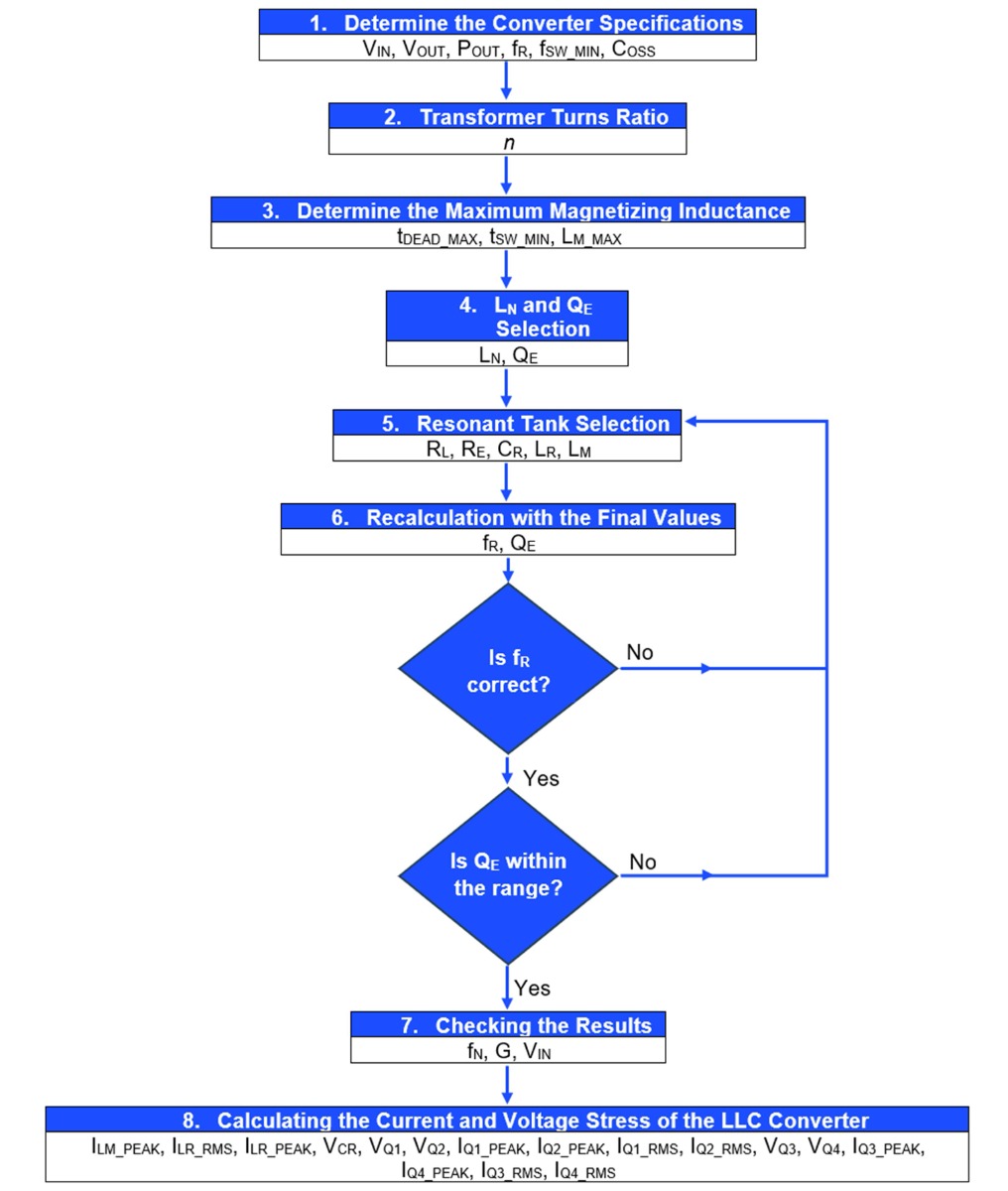
图 2:LLC 谐振变换器设计流程图
设计考量
LLC 谐振变换器的效率和性能受以下两个关键因素的显著影响:
- 优化谐振电感比LN):高 LN通常可提高重载条件下的效率。建议将 LN 保持在4至10的范围内,以平衡效率和元件应力。
- 选择适当的品质因数 QE):为了防止谐振电容上出现过大的电压应力,并最大程度地降低启动期间的大浪涌电流,QE需保持在0.34至0.49的范围内,以确保在最小化应力和保持变换器整体性能之间取得良好平衡。


步骤1:确定变换器规格
表 1 列出了示例 LLC 谐振变换器的规格。
表1:示例LLC谐振变换器规格
| 参数 | 值 | 单位 |
|---|---|---|
| 输入电压(VIN) | 400 | VDC |
| 输出电压(VOUT) | 48 | VDC |
| 输出功率(POUT) | 600 | W |
| 谐振频率(fR) | 100 | kHz |
| 最小开关频率(fSW_MIN) | 50 | kHz |
| MOSFET输出电容 | 80 | pF |
步骤2:计算变压器匝数比
在计算变压器匝数比(n)时,需设增益(G)为1,以确保系统工作在谐振频率(fR)下。通过公式(1)来计算n:
$$ n = \frac{N_1}{N_2} = \frac{V_{\text{IN}}}{2 \times V_{\text{OUT}}} \times G \Rightarrow n = \frac{400}{2 \times 48} \times 1 \Rightarrow n = 4.17 $$上式得出的n = 4.17 可以四舍五入为整数,即 nLLC = 4。
步骤3:确定最大磁化电感
计算最大磁化电感(LM_MAX)需首先确定以下参数:最大死区时间(tDEAD_MAX)、最小开关周期(tSW_MIN)和原边 MOSFET 的输出电容(COSS)。
本设计选用了MPS的增强型 LLC 控制器HR1002A。这款器件经验证在各种工作条件下均具有高可靠性。根据HR1002A数据手册,其tDEAD_MAX为2µs 。所选 MOSFET 的输出电容(COSS)为80pF 。
用公式(2)计算 tSW_MIN:
$$ t_{\text{SW_MIN}} = \frac{1}{f_{\text{START_UP}}} \Rightarrow t_{\text{SW_MIN}} = \frac{1}{3 \times f_{\text{SW}}} \Rightarrow t_{\text{SW_MIN}} = \frac{1}{3 \times 100\,\text{kHz}} \Rightarrow t_{\text{SW_MIN}} = 3.33\,\mu\text{s} $$用公式(3)计算 LM_MAX:
$$ L_{\text{M_MAX}} = t_{\text{MIN}} \times \frac{t_{\text{DEAD_MAX}}}{16 \times C_{\text{OSS}}} \Rightarrow L_{\text{M_MAX}} = 3.33\,\mu\text{s} \times \frac{2\,\mu\text{s}}{16 \times 80\,\text{pF}} \Rightarrow L_{\text{M_MAX}} = 5.2\,\text{mH} $$步骤 4:选择 LN 和 QE
依据前文提到的设计考量,建议在公式 (4) 所示的范围内考虑 QE 的取值:
$$ \frac{1}{3} < Q_E < \frac{1}{2} \Rightarrow 0.33 < Q_E < 0.5 $$此外,QE 还与谐振电容电压应力以及启动时的浪涌电流有关,因此选择 QE 值为0.35,接近最小值。
与 QE 类似,在公式(5)所示的范围内考虑 LN 的取值:
$$ 4 \leq L_N \leq 10 $$如果考虑在全负载范围内获得稳定的效率,建议 LN 取值在4至6之间;如果优先考虑最大输出功率(POUT)下的效率,则建议在6至10之间取值。在本例的 LLC 谐振变换器中,LN 定为9。
步骤5:选择谐振回路
选择谐振回路需要确定以下参数:负载电阻(RL)、等效负载电阻(RE)、谐振电容(CR)、谐振电感(LR)和磁化电感(LM)。
用公式(6)计算 RL:
\[ R_L = \frac{{V_{\mathrm{OUT}}}^2}{P_{\mathrm{OUT}}} \Rightarrow R_L = \frac{48^2}{600} \Rightarrow R_L = 3.84\,\Omega \]然后用公式(7)计算 RE:
\[ R_E = \frac{8 \times {n_{\mathrm{LLC}}}^2}{\pi^2} \times R_L \Rightarrow R_E = \frac{8 \times 4^2}{\pi^2} \times 3.84 \Rightarrow R_E = 49.8\,\Omega \]再用公式(8)计算 CR:
$$ C_R = \frac{1}{2 \pi \times f_R \times R_E \times Q_E} \Rightarrow C_R = \frac{1}{2\pi \times 100\,\mathrm{kHz} \times 49.8 \times 0.35} \Rightarrow C_R = 91.31\,\mathrm{nF} $$建议将 CR 四舍五入到最近的标准电容值,或并联电容以获得最接近的值。本例采用了两个并联的47nF电容,以获得94nF的总电容 。
用公式(9)计算 LR:
$$ L_R = \frac{1}{(2 \pi f_R)^2 \times C_R} \Rightarrow L_R = \frac{1}{(2 \pi \times 100\,\text{kHz})^2 \times 94\,\text{nF}} \Rightarrow L_R = 26.95\,\mu\text{H} $$得到的 LR = 26.95µH 可四舍五入为27µH 。
用公式(10)计算 LN:
$$ L_N = \frac{L_M}{L_R} \Rightarrow L_M = L_N \times L_R \Rightarrow L_M = 9 \times 27\,\mu\text{H} \Rightarrow L_M = 243\,\mu\text{H} $$再通过公式(11)检查 LM:
$$ L_M \leq L_{M\_MAX} \Rightarrow 243\,\mu\text{H} \leq 5.2\,\text{mH} $$步骤6: 利用 LR、CR 和 LM 的最终值进行再计算
用 LR、CR 和 LM 最终值通过公式(12)再计算谐振频率(fR):
$$ L_R = \frac{1}{(2 \pi f_R)^2 \times C_R} \Rightarrow 2 \pi f_R = \frac{1}{\sqrt{L_R \times C_R}} \Rightarrow f_R = \frac{1}{2 \pi \sqrt{L_R \times C_R}} $$ $$ \Rightarrow f_R = \frac{1}{2 \pi \sqrt{27\,\mu\text{H} \times 94\,\text{nF}}} \Rightarrow f_R = 99.9\,\text{kHz} $$用 LR、CR 和 LM 的最终值通过公式(13)再计算 QE:
\begin{align*} & C_R = \frac{1}{2 \pi \times f_R \times R_E \times Q_E} \Rightarrow Q_E = \frac{1}{2 \pi \times f_R \times R_E \times C_R} \Rightarrow Q_E = \frac{1}{2\pi \times 99.9\,\mathrm{kHz} \times 49.8 \times 94\,\mathrm{nF}} \\ & \phantom{C_R = \frac{1}{2 \pi \times f_R \times R_E \times Q_E}} \Rightarrow Q_E = 0.34 \end{align*}注意,QE 应在建议的取值范围内:
$$ 0.33 < Q_E < 0.5 \Rightarrow 0.33 < 0.34 < 0.5 $$如果 QE 超出指定范围,则调整 CR,然后重新利用公式 (8) 至公式 (13) 进行计算。
步骤7:检查结果
为验证计算结果,可利用 fN、G 和 VIN 来推导谐振回路的电压传递函数,进而验证 VOUT,以确保变换器正常工作。谐振回路特性和增益可以通过波特图来验证。
谐振回路电压传递函数
为了确保变换器在 fR下正常工作,先进行以下假设:
$$ f_N = \frac{f_{\text{SW}}}{f_R} = 1 \Rightarrow f_{\text{SW}} = f_R = 99.9\,\text{kHz} $$将上述参数应用于谐振回路电压传递函数,然后用公式(14)计算 G(fN):
\begin{aligned} G(f_N) &= \frac{1}{ \sqrt{ \left[ 1 + \frac{1}{L_N} - \frac{1}{f_N^2 \times L_N} \right]^2 + Q_E^2 \times \left( \frac{1}{f_N} - f_N \right)^2 } } \Rightarrow \\[10pt] G(1) &= \frac{1}{ \sqrt{ \left[ 1 + \frac{1}{9} - \frac{1}{1^2 \times 9} \right]^2 + 0.34^2 \times \left( \frac{1}{1} - 1 \right)^2 } } \Rightarrow G(1) = 1 \end{aligned}输出电压
输出电压 (VOUT) 可通过公式(15)计算得出:
$$ V_{\text{OUT}} = \frac{V_{\text{IN}}}{2 \times n_{\text{LLC}}} \times G \Rightarrow V_{\text{OUT}} = \frac{400}{2 \times 4} \times 1 \Rightarrow V_{\text{OUT}} = 50\,\text{V} $$单位增益下的 VOUT 为50V ,而不是48V 。
我们可以通过两种不同的方法来调节 VOUT。第一种方法是将增益降至低于1,可用公式(16)来计算:
$$ V_{\text{OUT}} = \frac{V_{\text{IN}}}{2 \times n_{\text{LLC}}} \times G \Rightarrow G = \frac{V_{\text{OUT}} \times 2 \times n_{\text{LLC}}}{V_{\text{IN}}} \Rightarrow G = \frac{48 \times 2 \times 4}{400} \Rightarrow G = 0.96 $$变换器工作于归一化开关频率(fN),其比率约为 1.2。fN可以通过求解方程 (14) 或绘制增益为 0.96的谐振回路波特图来找到(见图 4)。
用公式(17)计算 fSW:
$$ f_N = \frac{f_{\text{SW}}}{f_R} \Rightarrow f_{\text{SW}} = f_N \times f_R \Rightarrow f_{\text{SW}} = 1.2 \times 99.9\,\text{kHz} \Rightarrow f_{\text{SW}} = 119.88\,\text{kHz} $$由于组件公差,变换器通常在 fR 范围内工作,而不是在精确的 fR 下工作。
调节 VOUT 的第二种方法是改变输入电压 (VIN),可用公式 (18) 来计算:
$$ V_{\text{OUT}} = \frac{V_{\text{IN}}}{2 \times n_{\text{LLC}}} \times G(f_N) \Rightarrow V_{\text{IN}} = \frac{V_{\text{OUT}} \times 2 \times n_{\text{LLC}}}{G(f_N)} \Rightarrow V_{\text{IN}} = \frac{48 \times 2 \times 4}{1} \Rightarrow V_{\text{IN}} = 384\,\text{V} $$通过将 VIN 调至384V ,变换器可在 fR 下运行。
用波特图验证谐振回路和增益
验证计算结果的最有效方法是使用公式 (14) 绘制谐振回路电压传递函数波特图,并用公式 (16) 绘制增益波特图。我们考虑以下两种谐振回路增益场景。
第一种场景:VIN = 400V、LR = 27µH、CR = 94nF、LM = 243µH。下图展示了在 VIN = 400V 、增益为0.96时的谐振回路增益。
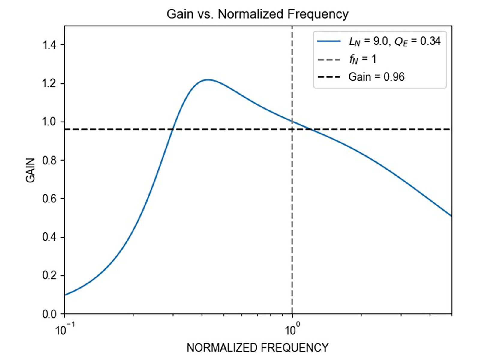
图 3:VIN = 400V、Gain = 0.96 和 fN = 1 时的谐振回路增益
在 fR 处,增益高于必要值。为了将增益降低至0.96,必须确定归一化频率(fN)。
图4显示了添加计算增益后的谐振回路增益。fN 比率为1.2,与0.96的增益相符(分别以灰色和黑色虚线表示)。
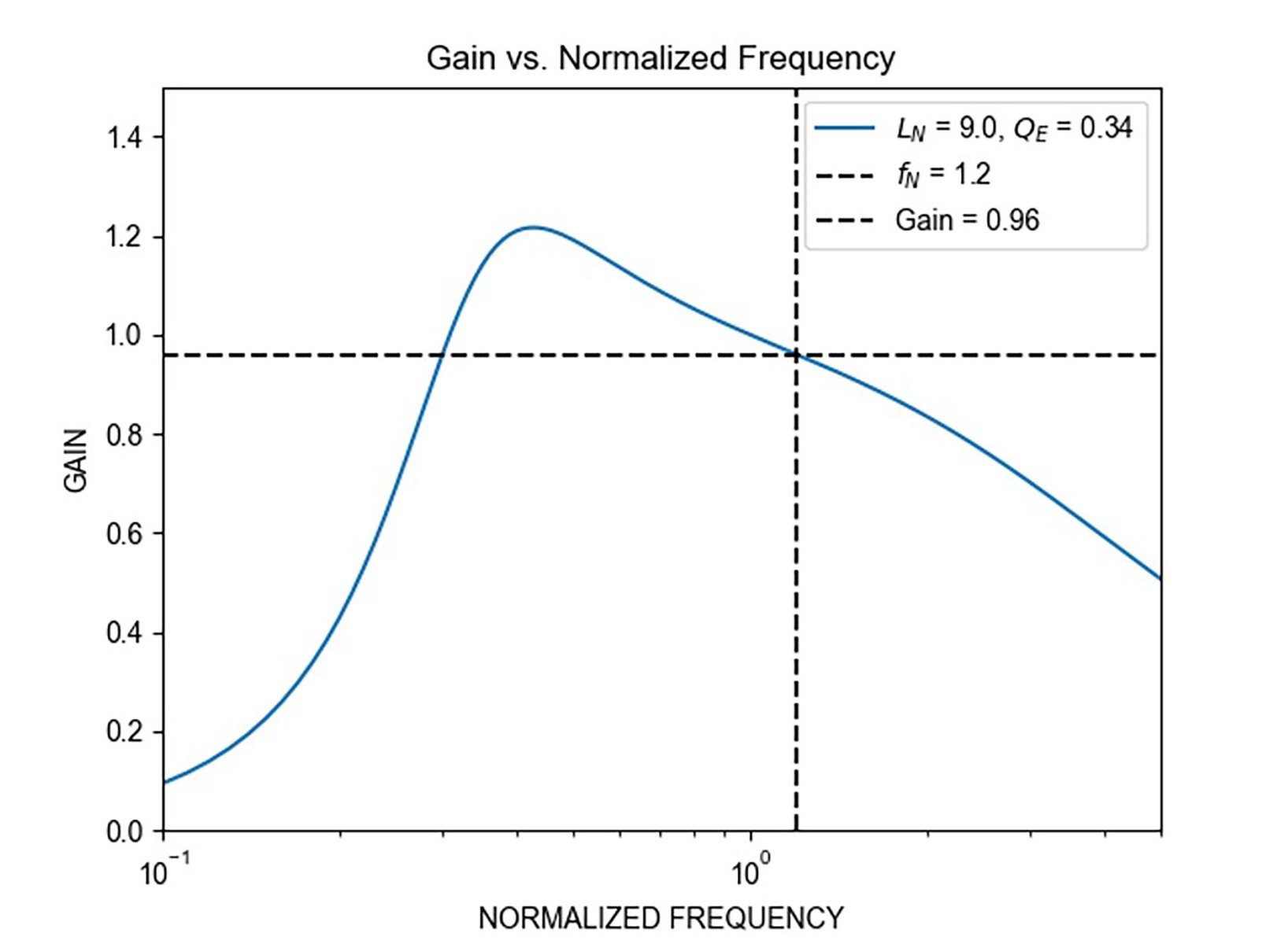
图 4:VIN = 400V、Gain = 0.96 和 fN = 1.2 时的谐振回路增益
第二种场景:VIN 降至384V,其他条件保持不变(LR = 27µH、CR = 94nF、LM = 243µH)。图5显示了 VIN = 384V 时的谐振回路增益,其中变换器以单位增益在 fR 下工作。
图 5:VIN = 384V 时的谐振回路增益
第二种场景适用于步骤 8 和最终设计,如下所述。
步骤8:计算LLC变换器的电流电压应力
LLC变换器的电流电压应力包括谐振回路应力、原边半导体器件应力和副边半导体器件应力。
谐振回路应力
谐振回路应力取决于磁化峰值电感电流(ILM_PEAK)、谐振电感 RMS 电流(ILR_RMS)、谐振峰值电感电流(ILR_PEAK)和谐振电容电压(VCR)。
ILM_PEAK 可用公式(19)来估算:
$$ I_{\text{LM_PEAK}} = \frac{n_{\text{LLC}} \times V_{\text{OUT}}}{4 \times L_M \times f_R} \Rightarrow I_{\text{LM_PEAK}} = \frac{4 \times 48}{4 \times 243\,\mu\text{H} \times 99.9\,\text{kHz}} \Rightarrow I_{\text{LM_PEAK}} = 1.98\,\text{A} $$ILR_RMS 可用公式(20)来计算:
\[ \begin{aligned} I_{\mathrm{LR\_RMS}} &= \frac{V_{\mathrm{OUT}} \times \sqrt{4 \times \pi^2 + {n_{\mathrm{LLC}}}^4 \times {R_L}^2 \times \left( \frac{1}{L_M \times f_R} \right)^2}}{4 \times \sqrt{2} \times n_{\mathrm{LLC}} \times R_L} \\ &= \frac{48 \times \sqrt{4 \times \pi^2 + 4^4 \times 3.84^2 \times \left( \frac{1}{243\,\mu\mathrm{H} \times 99.9\,\mathrm{kHz}} \right)^2}}{4 \times \sqrt{2} \times 4 \times 3.84} \\ &\Rightarrow I_{\mathrm{LR\_RMS}} = \mathbf{3.74\,\mathrm{A}} \end{aligned} \]ILR_PEAK 可用公式(21)计算:
$$ I_{\text{LR_PEAK}} = \sqrt{2} \times I_{\text{LR_RMS}} \Rightarrow I_{\text{LR_PEAK}} = \sqrt{2} \times 3.74 \Rightarrow I_{\text{LR_PEAK}} = 5.29\,\text{A} $$VCR 用公式(22)计算:
\begin{aligned} V_{CR} &= \frac{I_{LR\_RMS}}{2 \times \pi \times f_R \times C_R} \Rightarrow V_{CR} = \frac{3.74}{2 \times \pi \times 99.9\,\text{kHz} \times 94\,\text{nF}} \Rightarrow V_{CR} = 63.39\,\text{V} \end{aligned}原边半导体器件应力
原边半导体器件应力取决于原边电压应力(VQ1)、原边峰值电流(IQ1_PEAK)和原边RMS 电流(IQ1_RMS)。
VQ1 可用公式(23)来计算:
$$ V_{Q1} = V_{Q2} = V_{\text{IN}} = 384\,\text{V} $$IQ1_PEAK 用公式(24)来计算:
$$ I_{\text{Q1_PEAK}} = I_{\text{Q2_PEAK}} = I_{\text{LR_PEAK}} = 5.29\,\text{A} $$IQ1_RMS 用公式 (25) 计算:
\[ \begin{aligned} I_{\mathrm{Q1\_RMS}} = I_{\mathrm{Q2\_RMS}} &= \frac{V_{\mathrm{OUT}} \times \sqrt{4\pi^2 + {n_{\mathrm{LLC}}}^4 \times {R_L}^2 \times \left( \frac{1}{L_M \times f_R} \right)^2}}{8 \times n_{\mathrm{LLC}} \times R_L} \\ &= \frac{48 \times \sqrt{4\pi^2 + 4^4 \times 3.84^2 \times \left( \frac{1}{243\,\mu\mathrm{H} \times 99.9\,\mathrm{kHz}} \right)^2}}{8 \times 4 \times 3.84} \\ &\Rightarrow I_{\mathrm{Q1\_RMS}} = I_{\mathrm{Q2\_RMS}} = \mathbf{2.65\,\mathrm{A}} \end{aligned} \]高 LN 意味着高 LM 这会降低半导体器件中的 RMS 电流。
副边半导体器件应力
副边半导体器件应力取决于副边电压应力(VQ3)、副边峰值电流(IQ3_PEAK)和副边 RMS 电流(IQ3_RMS)。
VQ3 可用公式(26)来计算:
\[ V_{Q3} = V_{Q4} = 2 \times V_{\text{OUT}} \Rightarrow V_{Q3} = V_{Q4} = 2 \times 48 \Rightarrow V_{Q3} = V_{Q4} = 96\,\text{V} \]IQ3_PEAK 用公式(27)来计算:
\[ \begin{aligned} I_{\mathrm{Q3\_PEAK}} = I_{\mathrm{Q4\_PEAK}} &= \sqrt{12} \times \frac{V_{\mathrm{OUT}} \times \sqrt{12\pi^4 + \left( \frac{5\pi^2 - 48}{(L_M \times f_R)^2} \right) \times {n_{\mathrm{LLC}}}^4 \times {R_L}^2}}{24\pi \times R_L} \\ &= \sqrt{12} \times \frac{48 \times \sqrt{12\pi^4 + \left( \frac{5\pi^2 - 48}{(243\,\mu\mathrm{H})^2 \times (99.9\,\mathrm{kHz})^2} \right) \times 4^4 \times 3.84^2}}{24\pi \times 3.84} \\ &\Rightarrow I_{\mathrm{Q3\_PEAK}} = I_{\mathrm{Q4\_PEAK}} = \mathbf{19.71\,\mathrm{A}} \end{aligned} \]IQ3_RMS 用公式(28)计算:
\[ \begin{aligned} I_{\mathrm{Q3\_RMS}} = I_{\mathrm{Q4\_RMS}} &= \sqrt{3} \times \frac{V_{\mathrm{OUT}} \times \sqrt{12\pi^4 + \left( \frac{5\pi^2 - 48}{(L_M \times f_R)^2} \right) \times {n_{\mathrm{LLC}}}^4 \times {R_L}^2}}{24\pi \times R_L} \\ &= \sqrt{3} \times \frac{48 \times \sqrt{12\pi^4 + \left( \frac{5\pi^2 - 48}{(243\,\mu\mathrm{H})^2 \times (99.9\,\mathrm{kHz})^2} \right) \times 4^4 \times 3.84^2}}{24\pi \times 3.84} \\ &\Rightarrow I_{\mathrm{Q3\_RMS}} = I_{\mathrm{Q4\_RMS}} = \mathbf{9.85\,\mathrm{A}} \end{aligned} \]最终设计
一旦计算出谐振回路和半导体器件电流电压应力,基于HR1002A的LLC变换器设计就完成了。表2对设计结果进行了总结。
表 2:设计结果
| 参数 | 值 | 单位 |
|---|---|---|
| 输入电压 | 384 | V |
| 磁化电感 | 243 | µH |
| 变压器匝数比 | 4 | - |
| 谐振电感 | 27 | µH |
| 谐振电容 | 94 | nF |
| 峰值电流(Q1、Q2 和 LR) | 5.29 | A |
| RMS 电流(Q1、Q2 和 LR) | 2.65 | A |
| 谐振电容电压 | 63.39 | V |
| 峰值电流(Q3和Q4) | 19.71 | A |
| RMS电流(Q3和Q4) | 9.85 | A |
作为一款增强型 LLC 控制器,HR1002A 提供了强大的自适应死区时间调整 ( ADTA )功能以及多种保护功能,包括直通保护和避免硬开关的容性模式保护 (CMP)。此外,该器件还提供两级过流保护 (OCP) ,其中一级可通过配置延迟来增强浪涌抗扰能力。HR1002A 还可通过配置Brown-in和brownout过压/欠压阈值来设定变换器开始工作的最低输入电压(VIN)。
HR1002A 拥有的强大功能使功率转换级只需几个外部元件即可高效运行。
图6展示了采用 HR1002A 实现的带中心抽头变压器的半桥 LLC 原理图。
图6: 采用 HR1002A 实现带中心抽头变压器的半桥 LLC
结语
原边和副边 LLC 拓扑结构的选择对于优化应用性能至关重要。对功率水平高达 1kW 的应用而言,带中心抽头变压器的半桥 LLC 是理想之选。
遵循本文阐述的设计原则,包括优化谐振电感比和品质因数,工程师可确保变换器在所需的参数范围内运行,同时还能降低组件故障风险。凭借先进的保护功能,采用 HR1002A 控制器可进一步增强 LLC 变换器的设计性能,确保其在实际应用中的可靠性和耐用性。
如需了解更多解决方案选项,请浏览MPS 的集成型、高可靠性LLC 控制器产品页面。
_______________________
您感兴趣吗? 点击订阅,我们将每月为您发送最具价值的资讯!
技术论坛
 Latest activity 3 years ago
 9 回复
Latest activity 3 years ago
3 回复
Latest activity 3 months ago
10 回复
9 回复
Latest activity 3 years ago
3 回复
Latest activity 3 months ago
10 回复
直接登录
创建新帐号