满足阻抗容限要求:PDN设计与优化策略

简介
目标阻抗是电信应用中电源传输网络(PDN)设计的关键基准。通过定义芯片上电源轨的最大PDN阻抗,可确保芯片即使在最差的瞬态电流条件下,也能在可接受的电源轨电压噪声水平内运行。
本文将重点介绍如何利用MPQ8785负载点 (PoL) 器件实现目标阻抗的优化,同时为寻求优化PDN的设计人员提供有效建议和实用指导,助力实现可靠高效的电力传输。
定义目标阻抗
随着高频信号的兴起和电路板功率需求的不断提升,电源设计人员越来越重视能够高效为集成电路 (IC) 供电的无噪声配电。控制PDN在特定频段的阻抗是确保高速系统正常运行且满足性能要求的一种方法。该阻抗的估算方法通常为:将最大允许纹波电压除以最大预期电流阶跃负载。PDN目标阻抗(ZTARGET)计算公式如下 :
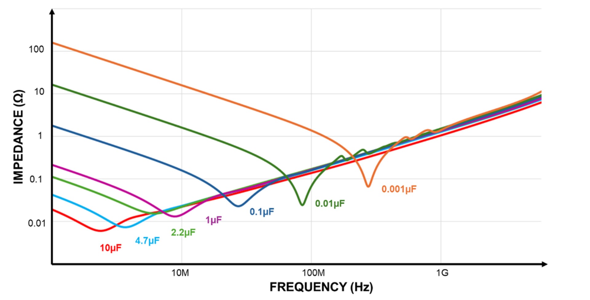
\[ Z_{\mathrm{TARGET}} = \frac{V_{\mathrm{SUPPLY}} \times \text{Ripple Tolerance}}{I_{\mathrm{TRANSIENT}}} \]实现宽频谱范围内的 ZTARGET 需要低频电源,并且在中高频段策略性地放置去耦电容。图 1 显示了多层陶瓷电容(MLCC)的阻抗频率特性。

图1:MLCC的阻抗频率特性
保持阻抗值始终低于计算出的阈值,就可以确保即使 IC 产生最严重的瞬态电流以及感应电压噪声,也能保持在可接受的操作范围内。
图 2 显示了不同频段的目标阻抗变化(数据来自供应商网站)。[1]可以看出,配电网中的每个元件都必须在不同频段下进行优化。
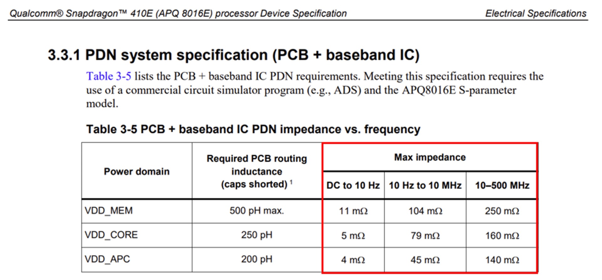
图2:目标阻抗示例
深入了解PDN 阻抗
理论上,电源轨应力求实现尽可能低的PDN阻抗。然而,要达到理想的零阻抗状态并不现实。在系统级芯片(SoC)下方布置多种去耦电容以压平全频率范围内的PDN阻抗,是一种广泛采用的降低PDN阻抗的策略。这种做法可有效抑制输出电压波动和信号抖动,但未必是优化电源轨设计的最有效方法。
三级低通滤波器法
要进一步优化电源轨设计,除了考虑实现最佳性能的新方法外,还需要重新审视PDN设计的基本原理。如图3所示,PDN可以概念化为三级低通滤波器,其中的每一级都在滤波和稳定SoC芯片电流方面发挥着特定的作用。

图3:将PDN概念化为三级低通滤波器
该三级低通滤波器具体描述如下:
- 从SoC晶片汲取电流:从SoC晶片汲取的任何电流都会首先经过封装滤波。封装与晶片侧电容(DSC)相互作用完成初始滤波,在电流到达PCB插座之前先降低其斜率。
- PCB布局与MLCC考量:电流通过 PCB 球栅阵列 ( BGA ) 后,会流经 PCB 上的电源层并遇到MLCC,此时发生第二级滤波。在此阶段,选择能够在特定频率下高效工作的电容非常关键。放置在 SoC 下方的高频电容对低频调节影响不大。
- 带电源层和大电容的电压调节器(VR):最后阶段涉及 VR 和大电容,二者共同作用,通过降低低频噪声来稳定电源。
PDN的三级滤波法能够确保每个组件都最大限度地降低不同频段的阻抗。这种结构化方法对于在现代电子系统中实现可靠高效的电力传输非常重要。


案例研究:电信评估板分析
下面我们通过一款MPS电信专用评估板做进一步的探讨。该评估板可演示高频同步降压变换器MPQ8785在实际环境中的功能。此外,本案例还强调了电容的选型和放置对于满足目标阻抗要求的重要性。
首先,在MPS评估板上提取PCB板寄生参数。如图4的MPQ8785评估板布局顶视图所示,选择两个端口进行分析。端口1位于电感后方,端口2连接至SoC BGA。
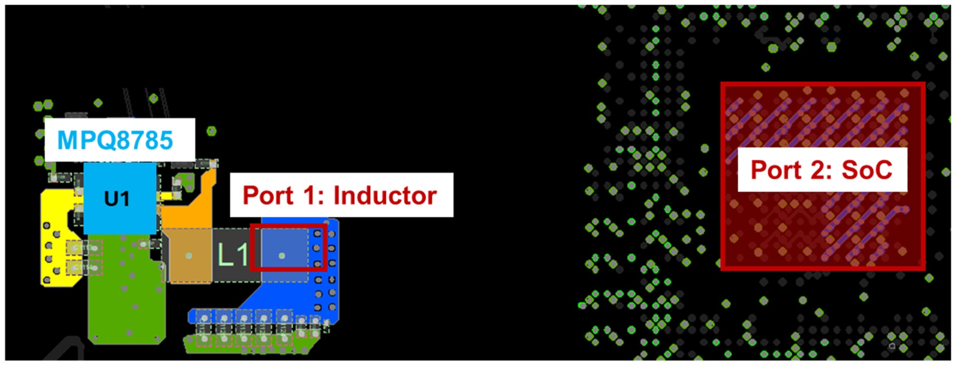
图4:MPS电信评估板
上图所示的电路板布局中包含了电容模型(来自供应商网站),其中已考虑等效串联电感(ESL)和等效串联电阻(ESR)等寄生参数。为保持阻抗曲线的平坦,我们在PCB底部 SoC下方尽可能多地布置了多种电容模型。
表1显示了针对不同频率,不同电容数量的初始选型方案。
表1:初始电容选型方案
| 数量 | 电容 |
|---|---|
| 2 | 560pF |
| 5 | 1nF |
| 2 | 0.01µF |
| 5 | 0.1µF |
| 2 | 1µF |
| 5 | 2.2µF |
| 2 | 4.7µF |
| 2 | 10µF |
| 3 | 22µF |
图5显示了核心轨PDN阻抗容限要求定义的目标阻抗曲线,与采用初始选定电容的MPQ8785评估板上实测初始阻抗的对比。图形化的对比能够直接评估阻抗特性,帮助判断PDN的性能表现。
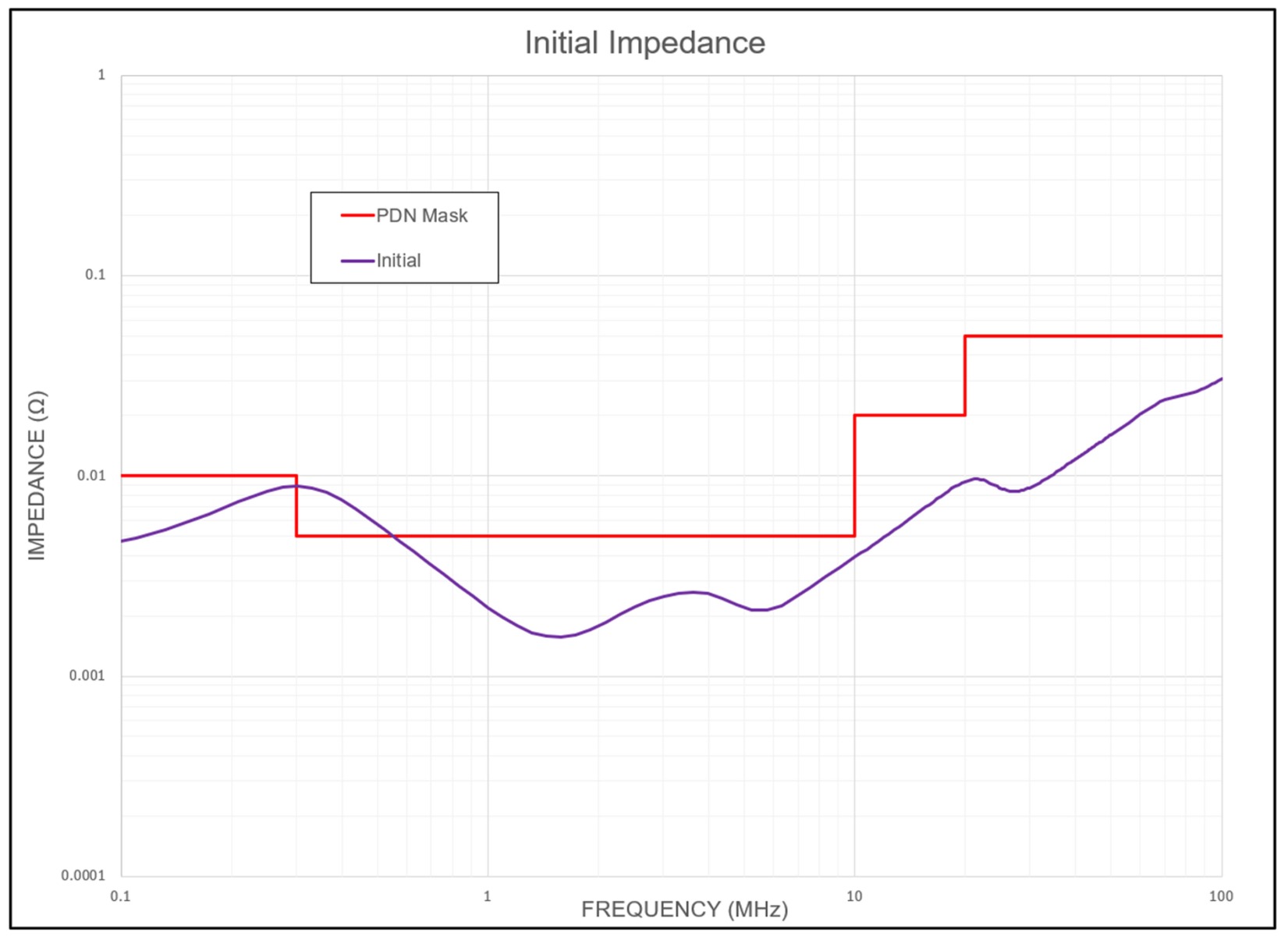
图5:目标阻抗曲线与初始阻抗的对比
根据图5可见,阻抗在300kHz至600kHz频段超出了规定限值,需要增加电容来缓解。引入额外电容可以有效降低该频段的阻抗,确保符合规范。需注意,高频电容对高频阻抗的影响几乎可以忽略不计,其影响仅限于特定的频率范围。这一点有助于优化电容选型,实现目标阻抗特性。
通过大量仿真实验,系统评估各种电容配置,即可成功确定满足阻抗容限要求的最佳电容组合。表2显示了经过迭代最终得到的最佳电容数量和总电容。
表2:最佳电容选型
| 数量 | 电容 |
|---|---|
| 5 | 10F |
| 5 | 22µF |
最终电容选型可确保PDN阻抗曲线符合规定的容限要求,从而保证可靠的电力传输和性能。图6所示为电容优化后的最终阻抗。
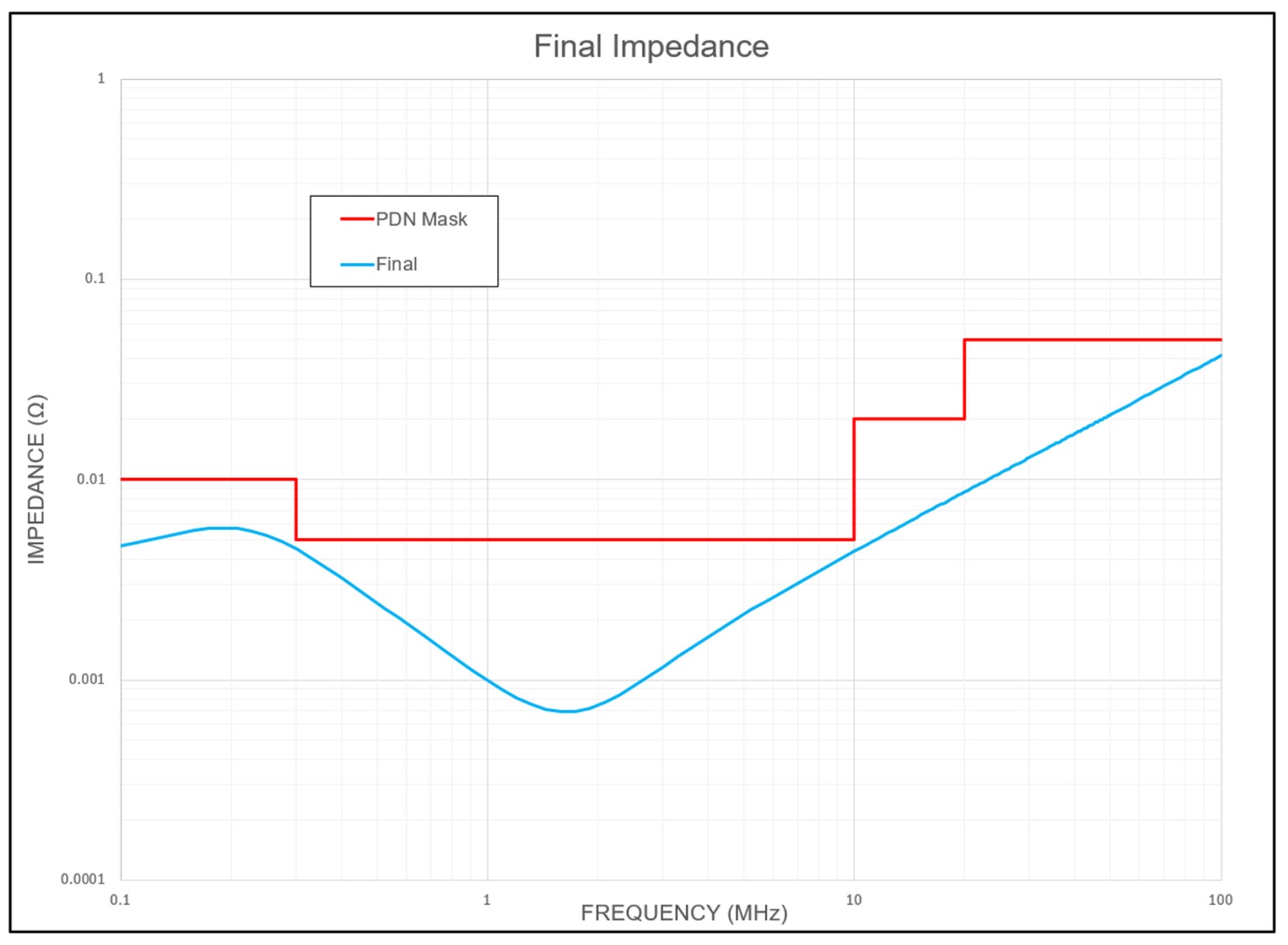
图6:电容优化后的最终阻抗
从上图可见,10MHz以上有充足的裕度,因此可省去主要影响高频的电容。这种策略性减少可以最大限度地减少占板面积并降低成本,同时确保符合所有规格。通过使用满足阻抗容限要求的最佳电容组合,可以有效地平衡性能、成本和占用空间,从而在整个工作频率范围内确保稳定的PDN功能。
为便于案例研究,我们在10MHz至40MHz频率范围内修改阻抗容限要求,将其总阻值降至10mΩ 。在评估板上额外添加10个0.1µF的电容能够降低阻抗,从而有效降低目标频段的阻抗。
图7显示了降低的阻抗容限要求以及评估板的阻抗响应。增加的电容成功降低了指定频段的阻抗。
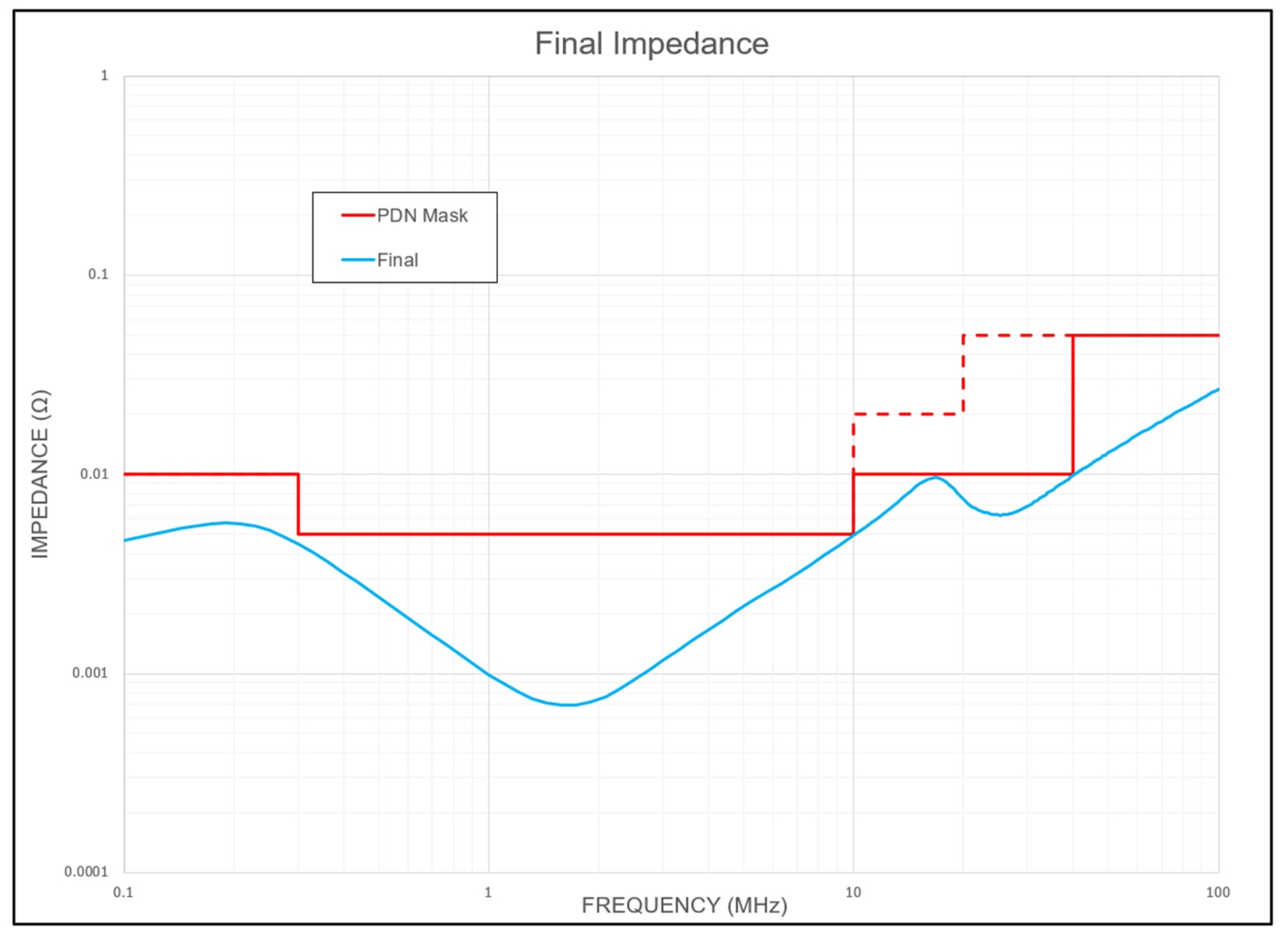
图7:电容优化后的阻抗,可降低PDN容限要求
结语
本文描述了如何利用MPQ8785评估板来优化 PDN 性能,确保其符合规定的阻抗容限要求。在优化过程中,我们建立模型来预测各种电容类型对不同频段阻抗的影响,从而为元件选型提供有效依据。
优化电容布局以减轻这些影响。
欲了解更多详细信息,请了解MPS的多款降压变换器产品。
参考资料
- Qualcomm Technologies, Inc., “Qualcomm® Snapdragon™ 410E (APQ 8016E) Processor Device Specification,” Section 3.3.1, Table 3-5, pp. 55, Sep. 2016.
_______________________
您感兴趣吗?点击订阅,我们将每月为您发送最具价值的资讯!
技术论坛
 Latest activity 4 days ago
 4 回复
Latest activity a year ago
24 回复
Latest activity a year ago
17 回复
4 回复
Latest activity a year ago
24 回复
Latest activity a year ago
17 回复
直接登录
创建新帐号