Analog Control Circuit Design Process
Analog control circuit design is a methodical process that necessitates careful component selection, a thorough understanding of the system requirements, and close attention to detail in order to guarantee reliable and efficient operation. This section gives engineering professionals and students an organized way to construct analog control circuits by outlining the key steps.
Define System Requirements
Objective: Clearly identify the control system's objectives and requirements.
Parameters: Establish the necessary input and output ranges, power consumption, accuracy, stability, response time, and environmental conditions.
Documentation: Make a thorough specification document that covers all of the limitations and needs for the system.
Develop the Control Strategy
Control Method: Based on the dynamic characteristics of the system and the desired performance, select a suitable control method (such as fuzzy logic, hysteresis, or proportional-integral-derivative, or PID).
Algorithm Design: Create the control algorithm and mathematical model, incorporating compensation and feedback methods.
Component Selection
Active Components: Select transistors, operational amplifiers, and other active components according to specifications such power ratings, input/output impedance, bandwidth, and gain.
Passive Components: To ensure accuracy and stability, select resistors, capacitors, and inductors with suitable values, tolerances, and temperature coefficients.
Specialized Components: Identify any specialized components, such as comparators, oscillators, and filters, and select them depending on performance requirements.


Circuit Schematic Design
Schematic Creation: Using Electronic Design Automation (EDA) software, develop the circuit schematic, making sure that every component is connected and referenced correctly.
Feedback Loops: Use feedback loops to ensure appropriate signal conditioning and isolation, as well as stability and accuracy.
Simulation and Optimization: Run early simulations of the circuit to ensure its functioning. Make the required changes to component values and configurations as you iterate the design.
Prototype Development
Breadboarding: To test the circuit in a real-world setting, build a prototype on a breadboard or with other prototyping techniques.
Testing and Debugging: Test thoroughly to find and fix any problems, such as noise, oscillations, or component failures. When required, modify the circuit designs and component values.
PCB Design and Layout
PCB Layout: Consider factors like trace routing, component position, signal integrity, and heat management while creating the Printed Circuit Board (PCB) layout.
Grounding and Shielding: Use appropriate shielding and grounding methods to reduce interference and noise.
Power Distribution: Make sure there is sufficient power distribution and decoupling to keep all components operating steadily.
Design Review
Peer Review: Conduct a design review with colleagues or specialists to discover potential improvements and ensure the design's robustness.
Final Testing and Validation
Prototype Testing: Verify the assembled PCB prototype's performance against the specified system requirements by testing it in a range of operating conditions.
Parameter Tuning: To maximize performance, fine tune the component values and control parameters.
Environmental Testing: To guarantee reliability under a variety of temperature, humidity, and vibration conditions, conduct environmental tests.
Documentation
Documentation: Assemble comprehensive documentation such as the user manual, test results, bill of materials (BOM), final schematic, and PCB layout.
Production and Deployment
Manufacturing: Make sure all components are available and up to quality standards before preparing the design for manufacturing.
Deployment: Install the final product in the specified application and offer assistance with calibration, maintenance, and installation.
Circuit Design Techniques and Best Practices
To create reliable and effective analog control circuits, best practices and proven design techniques must be followed. These techniques guarantee that the circuit operates as intended with excellent precision, stability, and low noise. In this section, important methods and best practices for designing analog control circuits are discussed, including component selection, layout considerations, and thermal management.
Feedback Loop Design
Principle: Achieving the required control performance, such as stability, accuracy, and dynamic response, requires well-designed feedback loops.
Techniques:
- Stability Margins: To prevent oscillations and ensure steady operation, maintain adequate phase and gain margins. To evaluate stability, use Bode plots and root locus analysis.
- Compensation: Improve system response and stability by implementing compensation techniques (such as lead, lag, and lag-lead).
- Error Amplification: For precise control action, use operational amplifiers in feedback loops to amplify error signals.
Component Matching
Principle: Accurate component selection and matching can greatly enhance circuit performance.
Techniques:
- Precision Components: To reduce errors brought on by component tolerances, use high-precision resistors, capacitors, and op-amps.
- Temperature Coefficients: For stable functioning at various temperatures, select components with low temperature coefficients.
Signal Conditioning
Principle: In control circuits, signal conditioning enhances the reliability and quality of input and output signals.
Techniques:
- Filtering: Utilize band-pass, notch, high-pass, and low-pass filters to eliminate unwanted noise and interference from signals.
- Amplification: Amplify signals appropriately to ensure the best possible signal-to-noise ratio by matching the input range of the subsequent stages.
Power Supply Design
Principle: The reliable operation of analog circuits depends on a clean and steady power supply.
Techniques:
- Decoupling Capacitors: To remove high-frequency noise, place decoupling capacitors near the active devices' power pins.
- Regulated Power Supplies: To keep voltage levels consistent in spite of variations in input and load voltage, use voltage regulators.
Grounding and Shielding
Principle: Accurate signal processing is ensured by proper grounding and shielding, which reduce noise and interference.
Techniques:
- Single-Point Ground: Avoid ground loops, which can cause noise, by using a single-point ground system.
- Shielded Cables and Enclosures: To safeguard sensitive signals from external electromagnetic interference (EMI), use shielded cables and enclosures.
PCB Layout
Principle: The performance of analog control circuits is significantly influenced by the PCB's physical layout.
Techniques:
- Component Placement: Organize components rationally to cut down on parasitic capacitance and inductance as well as trace lengths.
- Signal Traces: To prevent crosstalk and interference, keep signal traces short and route them away from high-power or high-frequency areas.
- Ground Planes: To lower impedance and give signals a steady reference, use continuous ground planes.
Best Practices
Simulation and Prototyping
Principle: Prior to physical implementation, simulate the circuit to find potential issues and maximize performance.
Techniques:
- SPICE Simulation: To validate the design and model the behavior of the circuit under different conditions, use simulation tools based on SPICE.
- Breadboarding: To test and improve the design in real-world conditions, construct a prototype using a quick-turn PCB or a breadboard.
Thermal Management
Principle: Longevity and reliable operation of the circuit components are guaranteed by efficient thermal management.
Techniques:
- Heat Sinks: To dissipate heat more efficiently, use heat sinks on power-hungry components.
- Thermal Vias and Planes: To improve heat dissipation, include copper planes and thermal vias in the PCB design.
Documentation and Review
Principle: Comprehensive documentation and peer evaluations enhance the design process and final product quality.
Techniques:
- Design Documentation: Keep thorough design documentation, including as test results, PCB layouts, and schematics.
- Design Reviews: To find potential issues and improvements perform regular design reviews with colleagues.
Robustness and Reliability
Principle: Circuits should be designed to be strong and reliable in a variety of operating conditions.
Techniques:
- Component Derating: To increase lifespan and reliability, operate components below their maximum ratings.
- Redundancy: To guarantee continuous operation in the event of component failure, implement redundancy in crucial areas.
Handling Noise and Interference in Analog Circuits
In analog circuit design, noise and interference pose serious challenges that affect control systems' accuracy, stability, and reliability. The optimal performance of analog circuits under a variety of operating conditions depends on the effective management of these challenges. The sources of noise and interference, how they affect analog circuits, and their solutions are examined in this section.
Sources of Noise and Interference
Thermal Noise
Principle: Generated by the random movement of electrons in resistive components.
Characteristics: Found in all resistive elements and increases with resistance and temperature.
Impact: Impacts low-level signal processing and limit the signal-to-noise ratio (SNR).
Shot Noise
Principle: This arises from the discrete character of electric charge in semiconductor devices.
Characteristics: Found in transistors, diodes, and other semiconductor components, aside from CMOS devices.
Impact: Impacts low-current applications and high-gain amplifier performance, and it is proportional to the current magnitude.
Flicker Noise (1/f Noise)
Principle: Has an inverse relationship with frequency and has an association with semiconductor devices.
Characteristics: Significant at lower frequencies.
Impact: Affects how well precision analog circuits, such as oscillators and low-frequency amplifiers, operate. At lower frequencies, flicker noise predominates, while at higher frequencies, thermal noise does.
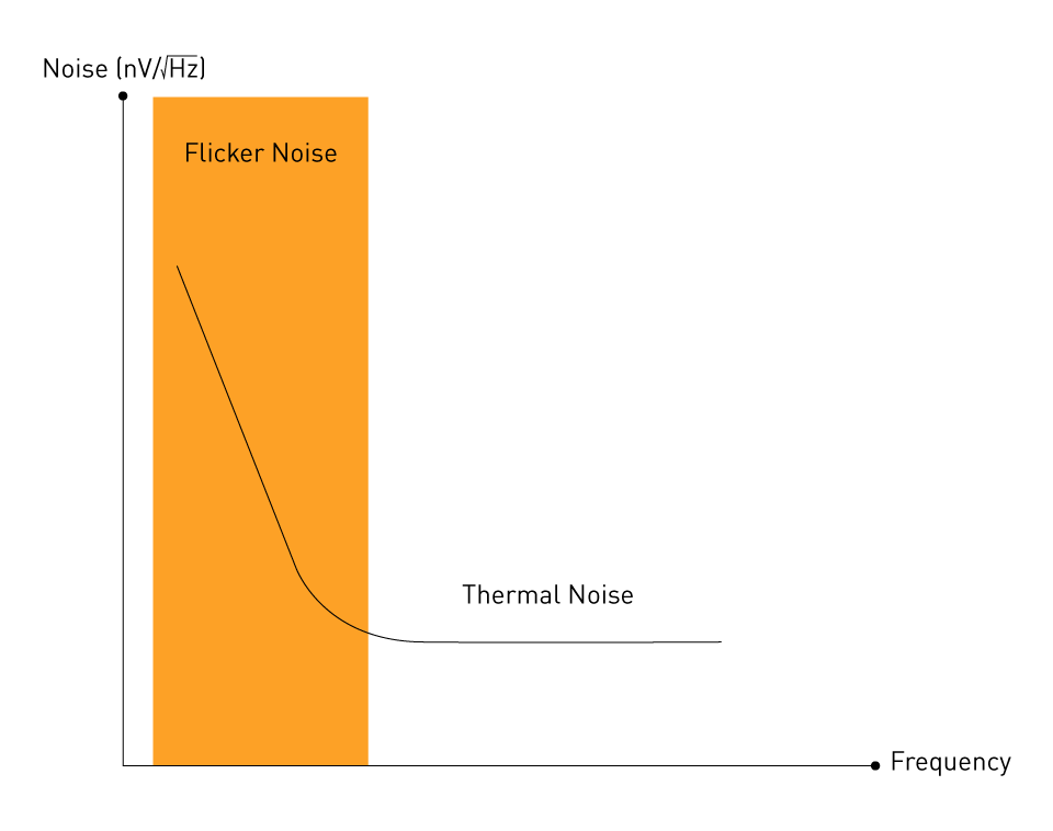
Figure 14: Impact of flicker and thermal noise vs. frequency
Electromagnetic Interference (EMI):
Principle: Caused by electromagnetic fields that come from external sources including motors, power lines, and communication equipment.
Characteristics: Can be radiated or transmitted, impacting circuit performance via inductive or capacitive coupling.
Impact: Causes undesired signals and noise, which may result in circuit malfunction or degradation.
Crosstalk:
Principle: Unintentional coupling between wires or signal traces.
Characteristics: Occurs as a result of shared routes and close proximity in PCB layout.
Impact: Causes signal integrity issues and inaccurate signal processing.
Mitigation Strategies
Shielding and Grounding:
Principle: While proper grounding reduces ground loops and offers a stable reference potential, shielding protects sensitive circuits from external electromagnetic interference(EMI).
Techniques:
- Shielded Cables: To stop radiated EMI from affecting the signals, use shielded cables for the signal lines.
- Ground Planes: To lower noise coupling and give return currents a low-impedance path, incorporate continuous ground planes in PCB designs.
- Chassis Grounding: To eliminate any potential differences and provide a common reference point, connect the circuit ground to the chassis ground.
Filtering:
Principle: Filters allow desired signals to get through while selectively attenuating undesirable noise frequencies.
Techniques:
- Low-Pass Filters: Use to improve signal integrity by attenuating high-frequency noise and harmonics.
- Band-Pass Filters: Limit the bandwidth of both signals and noise by selectively passing signals that fall inside a particular frequency range. Filters are useful in communication and sensor applications.
- Power Line Filters: Reduce conducted electromagnetic interference (EMI) from power supply by implementing filters at the power input.
Layout Considerations:
Principle: A properly designed PCB minimizes coupling and guarantees clean signal paths, which lowers noise and interference.
Techniques:
- Separation of Analog and Digital Grounds: To stop digital switching noise from influencing analog signals, isolate the analog and digital grounds.
- Short Signal Paths: Reduce the length of sensitive signal paths to reduce their exposure to noise sources.
- Trace Routing: To reduce inductive coupling and crosstalk, divert high-speed and high-current traces from sensitive analog signal paths.
Component Selection and Placement:
Principle: Noise generation and susceptibility are decreased by selecting the appropriate components and positioning them optimally.
Techniques:
- Low-Noise Components: For crucial signal paths, choose operational amplifiers, transistors, and resistors with low noise specifications.
- Bypass and Decoupling Capacitors: Capacitors can be placed near active components' power pins to reduce high-frequency noise and maintain power supply voltage.
Signal Averaging and Shielding Enclosures:
Principle: Random noise can be decreased by averaging multiple signal samples, while shielding enclosures protect circuits from external electromagnetic interference (EMI).
Techniques:
- Signal Averaging: To improve SNR in data acquisition systems, employ signal averaging techniques.
- Shielding Enclosures: To protect sensitive circuits from external electromagnetic fields, enclose them in conductive enclosures or metal.
Practical Examples of Analog Circuit Design
Understanding theoretical principles is crucial for building analog control circuits, but practical application cements this understanding. By illustrating how theoretical ideas are applied in real circuits, practical examples shed light on challenges and solutions faced in the real world. In order to demonstrate how design concepts and best practices can be used in diverse circumstances, this section explores a few of real-world analog circuit design examples.
Example 1: Temperature Control System
A temperature control system keeps an area, such a room or an industrial procedure, at the ideal temperature. This example shows how to use an operational amplifier to create a basic proportional-integral-derivative (PID) controller.
System Requirements:
Temperature Range: 0°C to 100°C
Accuracy: ±0.5°C
Response Time: < 2 seconds
Components:
Temperature Sensor: Thermistor (NTC type)
Op-Amps: LM741 or similar
Resistors and Capacitors: Various values for tuning the PID controller
Heater Element: Controlled by a transistor switch
Design Steps:
Sensor Signal Conditioning: The thermistor can be used with a voltage divider to generate a voltage that is proportional to the temperature.
PID Controller:
- Proportional Term: amplifies the error signal. Utilize an op-amp with a feedback resistor in a non-inverting configuration.
- Integral Term: Removes errors in steady state. Utilize an op-amp integrator circuit to integrate the error signal.
- Derivative Term: Predicts future errors, minimizes overshoot, dampens oscillations, and increases stability. Use an op-amp differentiator circuit to differentiate the error signal.
Combining PID Terms: Utilizing an additional op-amp configured as a summing amplifier, add the outputs of the three op-amp stages.
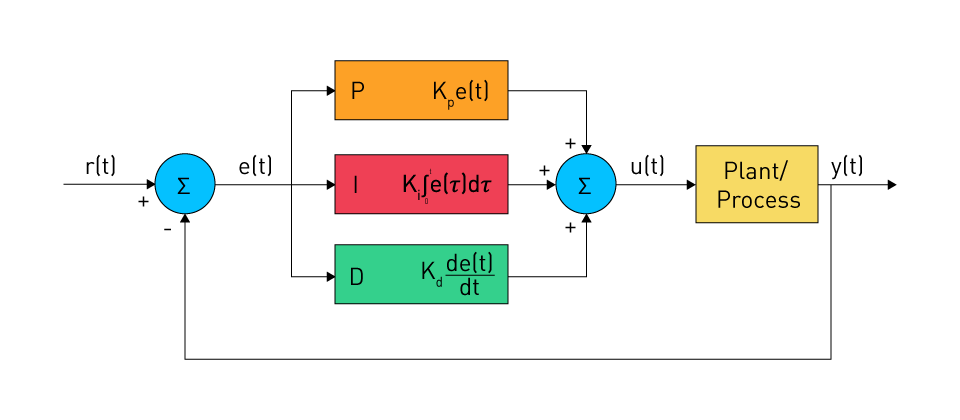
Figure 15: PID controller
Actuator Control: The heater element is controlled by a transistor switch that is driven by the combined PID output.
Testing and Tuning:
Prototype: Connect the temperature sensor and heater to the circuit after building it on a breadboard.
Tuning: To get the required accuracy and response time, modify the PID circuit's resistors and capacitors.
Example 2: Audio Equalizer
To improve sound quality in audio systems, an audio equalizer modifies the amplitude of audio signals in various frequency bands. This example shows how to create a three-band equalizer using active filter circuits.
System Requirements:
Frequency Bands: Low (20 Hz - 200 Hz), Mid (200 Hz - 2 kHz), High (2 kHz - 20 kHz)
Gain Control: ±12 dB adjustment for each band
Components:
Op-Amps: TL072 or similar low-noise op-amps
Resistors and Capacitors: Precision components for filter design
Potentiometers: For adjustable gain control
Design Steps:
Low-Pass Filter: For the low-frequency band, design a Sallen-Key low-pass filter.
Band-Pass Filter: Design a band-pass filter with multiple feedback for the mid-frequency band.
High-Pass Filter: Design a high-frequency band Sallen-Key high-pass filter.

Figure 16: Audio equalizer block diagram
Gain Control: To adjust the gain, use potentiometers in each filter stage's feedback loop.
Summing Amplifier: Utilizing an op-amp configured as a summing amplifier, combine the outputs of the three filter stages.
Testing and Calibration:
Prototype: Assemble the circuit properly on a PCB or breadboard.
Calibration: To get the desired gain control range for each frequency band, adjust the potentiometers.
Audio Testing: To verify performance, connect the equalizer to a speaker and an audio source. Then, test it using different audio signals.
Example 3: Power Supply Voltage Regulator
Regardless of variations in input voltage or load conditions, a voltage regulator keeps the output voltage constant. In this example, a pass transistor and an operational amplifier are used to design a linear voltage regulator.
System Requirements:
Input Voltage: 12 V ±10%
Output Voltage: 5 V ±0.1 V
Load Current: Up to 1 A
Components:
Op-Amp: LM358 or similar
Pass Transistor: NPN transistor (e.g., 2N3055)
Zener Diode: 5.1 V for reference voltage
Resistors and Capacitors: Various values for stability and filtering
Design Steps:
Reference Voltage: To get a stable 5.1 V reference voltage, use a Zener diode.
Error Amplifier: To compare the output voltage to the reference voltage, use an op-amp. The pass transistor is controlled by the error signal.
Pass Transistor: The transistor regulates the current to ensure a constant output voltage.
Output Filtering: Reduce noise and voltage ripple by adding capacitors to the output.

Figure 17: Voltage regulator
Testing and Adjustment:
Prototype: Connect the circuit to a variable load after building it on a breadboard.
Adjustment: To get the desired output voltage and stability, fine-tune the resistor values.
Load Testing: To make sure the regulator maintains a steady output voltage, test it with various load currents.
直接登录
创建新帐号