Basics of EMC and Why It Matters in Power Electronics
Electromagnetic compatibility (EMC) is an important factor in the design and operation of power electronic systems. The ability of electrical and electronic systems to operate properly in their electromagnetic environment without causing electromagnetic disturbances that disrupt the operation of other systems is known as electromagnetic compatibility (EMC). Achieving EMC is crucial in power electronics, where high voltages, switching transients, and rapidly fluctuating currents are frequent. This ensures that devices function reliably and safely without causing or experiencing interference from external sources.
Importance of EMC in Power Electronics
Power electronics convert, regulate, and control electrical power by using semiconductor devices such as thyristors, diodes, and transistors. Significant electromagnetic noise is generated by the fast switching of these devices, especially in high-power applications like power supplies, motor drives, and inverters. In the absence of proper EMC measures, this noise may radiate into the surrounding environment or couple into nearby circuits, resulting in undesired outcomes including data corruption, signal distortion, and sensitive equipment malfunction.
In power electronics, EMC is important for several reasons:
Operational Reliability: Power line disruptions, wireless communication signals, and nearby electronic devices are examples of external electromagnetic sources that could interfere with a power electronic system if it is not properly designed. Similarly, the system itself may produce electromagnetic noise that disrupts neighboring systems and compromise reliability.
Regulatory Compliance: The limits of electromagnetic emissions and immunity are established by international standards such as IEC 61000-4 (for EMC testing procedures) and CISPR 11 (for industrial, scientific, and medical equipment). Power electronic products must adhere to these standards to be sold and used legally in various regions.
Preventing System Failures: Conducted emissions, transient voltage spikes, and radiated emissions are examples of EMC-related issues that can cause system failures or performance degradation. Uncontrolled emissions, for instance, can interfere with communication systems, introduce noise to control signals, or even cause an unplanned power electronic system shutdown.
Ensuring Coexistence of Devices: In modern environments where multiple electronic devices operate at the same time, achieving EMC is critical for allowing devices to coexist without interference. For instance, communication devices, power supplies, and inverters frequently share a physical space or electrical network, and poor EMC design in one device might cause issues in other equipment.
Design Techniques for EMC Compliance
EMC compliance in power electronics necessitates the use of both active and passive control techniques to manage electromagnetic emissions and vulnerability. These design strategies shield sensitive circuits from external interference and reduce the generation of electromagnetic noise.
Use of EMI Filters
In power electronic systems, EMI filters are a common and effective method for controlling both conducted and radiated emissions.
EMI Filters: High-frequency noise is blocked by electromagnetic interference (EMI) filters in the input and output stages of power electronic devices. Typically, these filters consist of various configurations of inductors and capacitors arrangements that attenuate high-frequency signals while allowing low-frequency power to flow through.
Common-Mode Chokes: Common-mode noise that propagates along a power system's live and neutral lines can be suppressed with common-mode chokes. These chokes operate by allowing differential-mode signals to flow through while providing common-mode signals a high impedance.
Capacitors and Inductors: To attenuate high-frequency noise on AC or DC power lines, EMI filters frequently employ X-capacitors (across the line) and Y-capacitors (from line to ground). These capacitors operate in combination with inductors to provide low-pass filters, which allow low-frequency power through while blocking high-frequency noise.
Ferrite Beads: Ferrite beads are another effective and simple technique for decreasing high-frequency noise in power circuits. Placed on signal or power lines, ferrite beads provide resistive impedance at high frequencies, dampening high-frequency oscillations and minimizing conducted emissions.
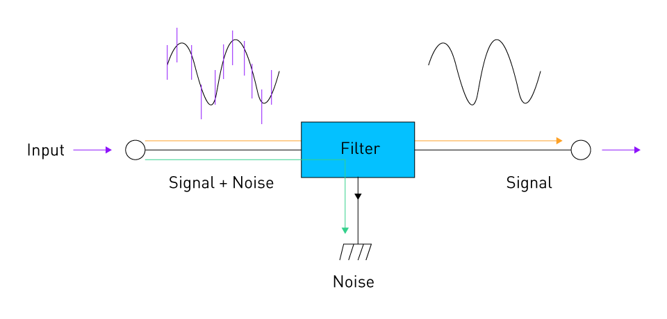
Figure 6: EMI filtering
Shielding and Enclosures
Physical shielding may be necessary for power electronics systems that generate significant radiated electromagnetic interference to comply with EMC regulations. In addition to shielding the internal circuits from external electromagnetic disturbances, shielding prevents electromagnetic fields from escaping the enclosure and interfering with neighboring systems.
Metal Enclosures: Conductive metal enclosures, such as steel or aluminum housings, operate as Faraday cages, efficiently blocking radiated emissions from escaping and shielding sensitive internal circuits from external EMI. The enclosure should be properly grounded for optimal performance, and joints and seams should be minimized to prevent gaps that allow EMI leakage.
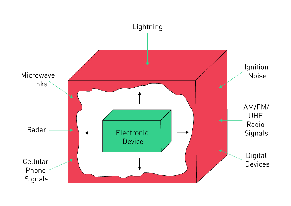
Figure 7: Shielding protection
Cable Shielding: Signal and power cables should be shielded in addition to the device itself, particularly in high-frequency applications. Shielded cables with grounded exterior conductors limit the amount of noise that can couple to the cable and radiate into the environment. For long cable runs in industrial or automotive systems, this is especially important.
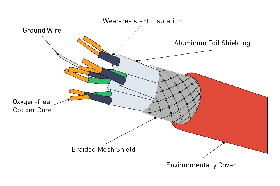
Figure 8: Shielded cable
PCB Layout Techniques
Effective printed circuit board (PCB) design is critical for managing electromagnetic emissions and guaranteeing immunity. Signal coupling, noise propagation, and radiated emissions can all be caused by poor PCB layout. Designers must adhere to several essential guidelines to minimize these issues:
Component Placement: Component placement on the PCB can enhance overall EMC performance and lower the generation of electromagnetic noise. To reduce noise coupling across long traces, high-frequency components such as drivers and switching transistors should be placed close to the power devices they manage.
Minimizing Loop Areas: Large EMI is often produced by high-frequency switching circuits, particularly those found in power converters, if current loops are not kept to a minimum. Radiated emissions can be decreased by decreasing the loop area on essential paths, such as between the switching transistor to the load.
Grounding Strategies: Achieving EMC compliance requires a well-designed ground plane. High-frequency signals should have a low-impedance return path from the ground plane. One useful tactic for avoiding ground loops is star grounding, in which multiple ground points converge at one location. Analog and digital grounds should be separated in high-power systems to avoid noise from digital switching circuits coupling into sensitive analog circuits.
Shielding Sensitive Traces: High-frequency traces, such as those carrying pulse-width modulation (PWM) or clock signals, can cause or be vulnerable to EMI. Reducing emissions and enhancing signal integrity can be achieved by routing these traces in differential pairs or over the ground plane.
Switching Transient Control
In power converters, switching transients or spikes are a major cause of electromagnetic interference (EMI), particularly when high-speed switching components such as MOSFETs and IGBTs are used. These devices' rapid switching generates high-frequency harmonics that can radiate or conduct through power lines. Switching-related EMI can be reduced using several strategies:
Snubber Circuits: To reduce voltage spikes across switching devices, snubber circuits are often used in motor drives and switching power supplies. A typical snubber consists of a resistor and capacitor placed across the switch to absorb high-frequency transients and limit the rate of voltage change (dv/dt).

Figure 9: Snubber circuit for transient voltage suppression
Soft Switching: In traditional hard-switching converters, abrupt variations in voltage and current during switching events produce electromagnetic noise. By ensuring that switching happens when the current or voltage is at or close to zero, soft switching techniques such as Zero-Current Switching (ZCS) and Zero-Voltage Switching (ZVS) decrease switching losses and electromagnetic noise. Lower electromagnetic emissions and increased system efficiency result from this.
Table 8: Hard- vs soft-switching
| Feature | Hard Switching | Soft Switching |
|---|---|---|
| Switching Losses | Higher losses due to abrupt transitions | Lower losses, smooth transitions |
| Efficiency | Lower efficiency due to energy dissipation | Higher efficiency, reduced heat generation |
| Circuit Complexity | Simpler design, fewer components | More complex, requires additional components |
| Heat Generation | Higher heat generation due to switching losses | Reduced heat generation |
Gate Drive Optimization: The rate at which a switching device switches on or off (determined by the gate driver) has a direct impact on EMI. Although switching losses are increased, EMI can be decreased by lowering the gate drive speed, which also lowers the rate of change of voltage (dv/dt) and current (di/dt). As a result, gate drive speed needs to be meticulously calibrated for efficiency and EMI control.
Impedance Matching and Termination
Impedance mismatches between the source, transmission line, and load in high-speed digital circuits can result in signal reflections, which can compromise signal integrity and lead to electromagnetic interference (EMI). By minimizing signal reflections, proper impedance matching reduces EMI.
Termination Resistors: Termination resistors can be added to the receiving end of transmission lines in high-speed signal lines to match the line's impedance, eliminating reflections and lowering radiated emissions. This is especially important for digital communication protocols that are frequently utilized in power electronics systems, such as CAN, Ethernet, and RS-485.
Controlled Impedance PCBs: The PCB stack-up for high-frequency signal traces must be meticulously designed to regulate the traces' impedance. Altering the trace width, the distance between the trace and the ground plane, and the PCB's dielectric material can accomplish this.
Power Supply Decoupling
Reducing conducted and radiated emissions requires power supply decoupling, especially in digital circuits with high-speed switching. C Decoupling capacitors placed between power and ground near the ICs serve to filter out high-frequency noise and stabilize the supply voltage.
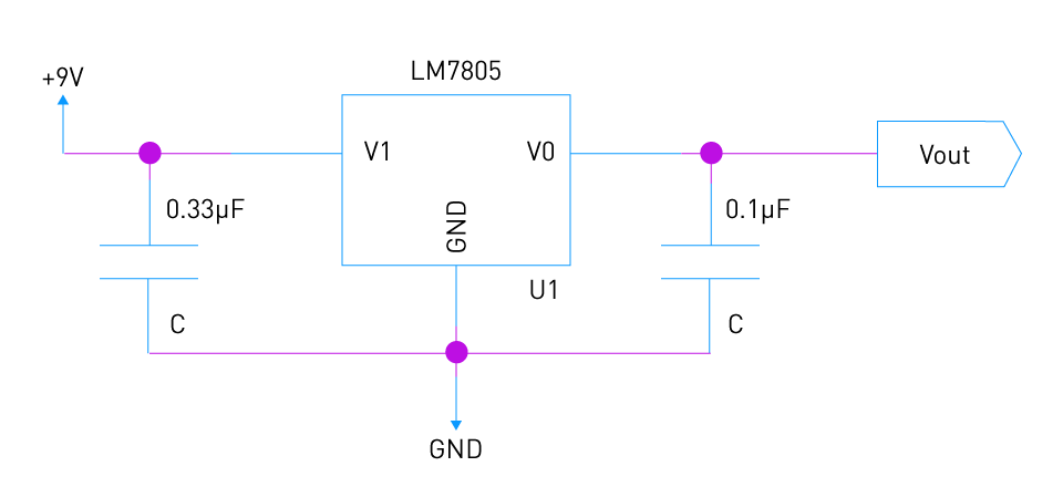
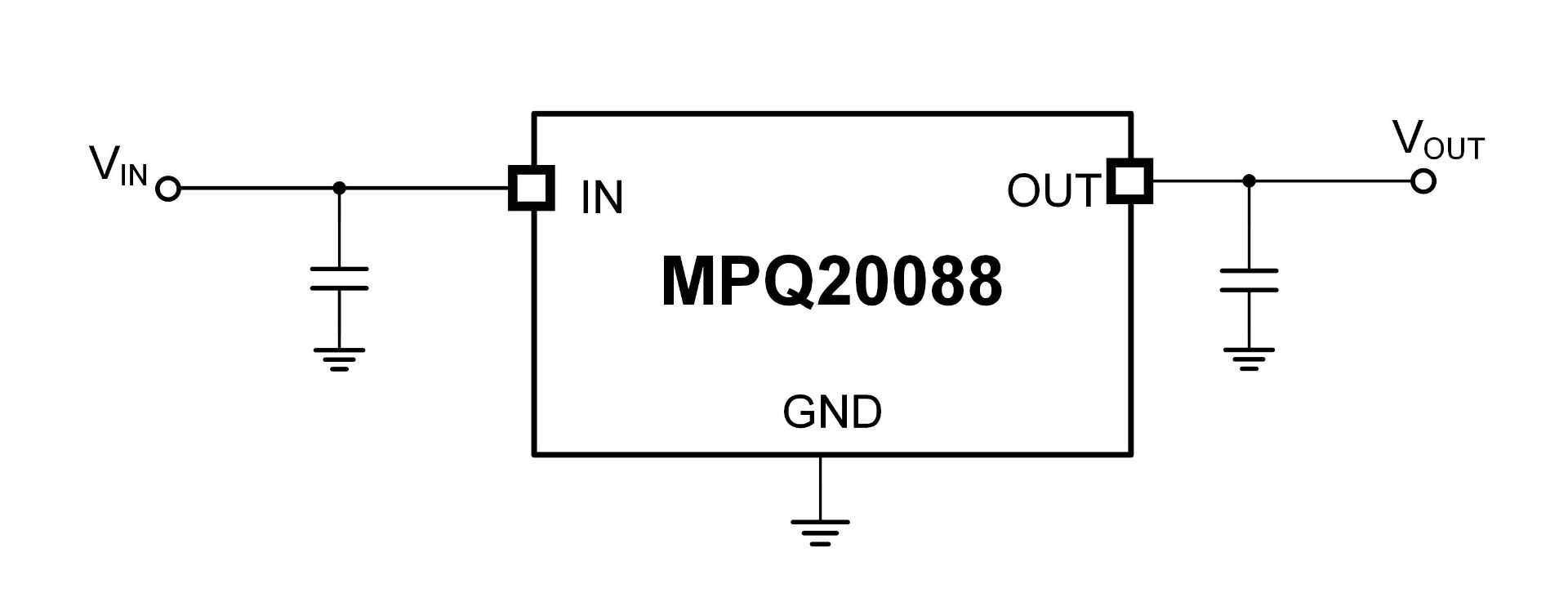
Figure 10: Linear voltage regulator with 2 decoupling capacitors
Bypass Capacitors: Placing bypass capacitors near IC power pins (usually between 0.1 µF and 10 µF) lowers high-frequency noise on the power rails. For high-frequency decoupling, low-inductance surface-mount capacitors are preferred.
Bulk Capacitors: Bulk capacitors, with larger capacitance values ranging from 10 µF to 1000 µF, are used to store energy locally and smooth out lower-frequency changes in the power supply. These capacitors aid to decrease power supply ripple, which can contribute to EMI if not properly filtered.
Spread Spectrum Techniques
Spread Spectrum Modulation includes changing the switching frequency of power converters over a wide range of frequencies rather than employing a fixed frequency. Peak emissions at any specific frequency are decreased by spreading electromagnetic energy over a broader spectrum, allowing the system to meet the emission limits specified by EMC standards.
Compliance with EMC Standards and Pre-Compliance Testing
Lastly, power electronic systems must be designed in accordance with international EMC standards, including FCC Part 15, IEC 61000, and CISPR. The risk of non-compliance during formal testing is decreased when these standards are considered during the design process. Early detection of any EMC issues by pre-compliance testing during the design stage enables designers to make the required modifications prior to undergoing full compliance testing.
Standards and Testing Procedures for EMC Compliance
Both the devices' reliability and legal marketability rely on power electronic products complying with electromagnetic compatibility (EMC) requirements. EMC standards define a device's immunity to external interference and set specific limits on electromagnetic emissions. Rigorous testing procedures are usually used to verify compliance with these standards. Following EMC regulations ensures that products can operate reliably even when there are external electromagnetic disturbances present, in addition to ensuring that they do not emit hazardous electromagnetic interference (EMI).
Key EMC Standards for Power Electronics
Guidelines for managing electromagnetic emissions and susceptibility in electronic devices have been developed by several international standards organizations. Some of the most frequently cited EMC standards that are relevant to power electronics are as follows:
International Special Committee on Radio Interference (CISPR):
CISPR 11: Defines the limits and techniques of measuring radio disturbance characteristics for medical (ISM), industrial, and scientific equipment. Industries that produce power electronic devices such as industrial controls, converters, and inverters extensively use it.
CISPR 22 (now replaced by CISPR 32): Addresses the testing techniques and limitations for information technology devices. It applies to power supplies in computing and communication devices, ensuring that emissions are within acceptable levels.
CISPR 14-1: Focuses on tools, home appliances, and related gadgets, establishing emission limits for products such as motor controls and power tools.
International Electrotechnical Commission (IEC):
IEC 61000-4-2 to IEC 61000-4-6: Electrical fast transients (EFT), electrostatic discharge (ESD), surge immunity, and conducted and radiated disturbances are among the electromagnetic immunity testing techniques covered by these standards. To ensure they can withstand external electromagnetic interference without malfunctioning, power electronic devices are tested against these standards.
IEC 61000-3-2: Defines limits for electrical devices' emissions of harmonic current. This is especially important for power supplies and converters, as harmonics can affect both the product and the power grid.
EN 55032:
It is a European standard imposing restriction on conducted and radiated emissions and replaces CISPR 22 for multimedia equipment. It is often applied to power electronics used in computing devices, audiovisual systems, and telecommunications equipment.
FCC Part 15 (United States):
This collection of regulations establishes acceptable emission levels for both consumer and commercial devices and regulates radio frequency (RF) devices. Before a device can be sold in the United States, it must be certified as compliant.
MIL-STD-461:
The standards for controlling electromagnetic emissions and susceptibility in military electronic systems are outlined in this U.S. military standard. Despite being developed for military applications, this standard is frequently applied in high-reliability industries such as defense and aerospace.
Testing Procedures for EMC Compliance
Emissions testing and immunity testing are the two main categories of EMC testing. While immunity tests verify that a device can operate normally even in the face of external electromagnetic noise, emissions tests ensure that a device doesn't generate excessive electromagnetic disturbances.
Emissions Testing:
Conducted Emissions: Electromagnetic disturbances that propagate along electrical cables, including power supply lines, are referred to as conducted emissions. To test for conducted emissions, the noise generated by the device through its cables must be measured and maintained within specified limits. Limits and testing techniques for conducted emissions are defined by the CISPR 11 and CISPR 32 standards. Typically, a line impedance stabilization network (LISN) is used to measure noise at specific frequencies.
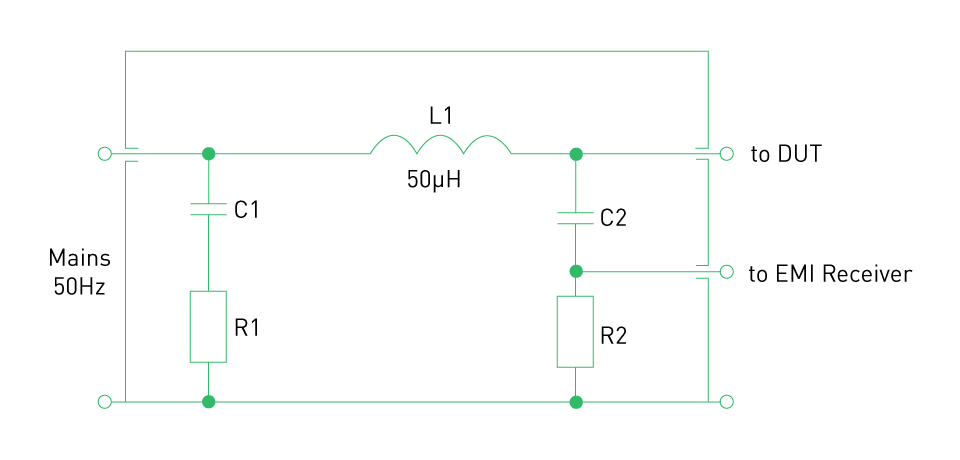
Figure 11: LISN circuit
Radiated Emissions: Electromagnetic waves that propagate through the air from the device are known as "radiated emissions." The testing technique involves placing the devices in an anechoic chamber or open-area test site and measuring electromagnetic field strength utilizing antennas. To ensure it doesn't interfere with adjacent electronic devices or communication systems, the device must comply with the radiated emissions restrictions specified in standards such as CISPR 32 and EN 55032.
Table 9: Emissions vs. immunity testing
| Feature | Emissions Testing | Immunity Testing |
|---|---|---|
| Purpose | Measures the electromagnetic energy emitted by a device | Tests how well a device withstands external electromagnetic interference |
| Focus | Ensures the device does not interfere with other equipment | Ensures the device continues to function properly under external interference |
| Test Environment | Involves measuring radiated and conducted emissions | Involves exposing the device to various electromagnetic fields or disturbances |
| Objective | Comply with emission limits set by regulations | Confirm the device’s resilience against external disturbances |
Immunity Testing:
Electrostatic Discharge (ESD): ESD testing assesses the device's ability to withstand abrupt discharges of static electricity, which might occur when operators or surrounding objects accumulate charge and touch the device. To verify that the device can withstand touch and air discharges without failure, the IEC 61000-4-2 standard specifies test techniques using ESD simulators.
Electrical Fast Transient (EFT) and Surge Immunity: Fast transient pulses and surge voltages are applied to power electronic devices to simulate real-world disruptions such as switching surges, lightning strikes, or motor start-up. The IEC 61000-4-5 (surge immunity) and IEC 61000-4-4 (EFT) standards outline how to test the device's resilience to these events, ensuring that it can continue to operate without experiencing malfunctions or performance degradation.
Radiated and Conducted Immunity: These tests assess the device's capacity to function in the presence of external electromagnetic fields or conducted disturbances to power and signal lines. IEC 61000-4-3 (radiated immunity) and IEC 61000-4-6 (conducted immunity) are two examples of standards that outline how to test equipment for electromagnetic interference from nearby sources and ensure they continue to function reliably.
Harmonics and Flicker Testing:
Harmonics Testing: Devices that draw current from the power grid can cause harmonic distortion, which affects the device's and the grid's stability and performance. Power electronic devices must not introduce excessive harmonics into the electrical supply, as defined by IEC 61000-3-2, which also establishes limits for harmonic current emissions. Harmonics testing is especially crucial for equipment that produces large harmonic distortion, such as switch-mode power supplies (SMPS) and motor drives.
Voltage Flicker: Power electronics can also cause fluctuations in the power supply voltage, which is known as flicker. The procedures for verifying voltage fluctuations caused by the device to ensure they stay within acceptable limits are outlined in IEC 61000-3-3.
Pre-Compliance Testing:
Pre-compliance testing is often carried out during the design process of a product to find and address possible EMC issues before it undergoes full EMC certification. Before submitting the product for final certification, pre-compliance tests are typically carried out in a less formal laboratory environment with the goal of finding emissions and immunity issues that can be resolved.
Full-Compliance Testing:
Full compliance testing must be carried out in a certified laboratory equipped with appropriate test conditions, such as anechoic chambers, reverberation chambers, or open-area test locations. The device's compliance with the relevant EMC standards is certified by the test results, allowing its sale in regulated markets. To receive regulatory approval from organizations such as the FCC, CE, or UL, this testing is especially crucial.
Troubleshooting EMC Issues in Power Electronic Products
Ensuring electromagnetic compatibility (EMC) in power electronic products is critical for their reliable and safe operation in environments where electromagnetic interference (EMI) can damage performance or disrupt other devices. Many power electronic systems experience EMC issues during development or after deployment, even with meticulous design. Identifying the underlying causes for excessive emissions or vulnerability to external electromagnetic interference (EMI) and implementing targeted solutions are necessary steps in troubleshooting these issues. The following are typical methods and techniques for resolving EMC issues in power electronic products.
Types of EMC Issues
Two categories of EMC issues commonly affect power electronic products:
Conducted emissions: These are undesired noises or signals that can disrupt other equipment by propagating along power or signal lines. According to EMC standards such as CISPR 22 and IEC 61000-6-3, conducted emissions are measured within specific frequency ranges.
Radiated emissions: These happen when electromagnetic noise is released into the environment directly from the power electronics circuits or associated components, frequently through inadequately grounded enclosures or unshielded cables.
Systems may also experience immunity issues, making them vulnerable to external electromagnetic interference (EMI) from other devices. It is necessary to enhance the system's ability to reject or tolerate interference in these cases.
Systematic Troubleshooting Process
Effective troubleshooting of EMC issues needs a systematic approach to detecting the cause of the problem and adopting corrective measures. The following steps outline the process:
Pre-Compliance Testing:
Prior to official EMC compliance testing, pre-compliance testing allows designers to find EMC issues early in the design process. To identify emissions and susceptibility issues, this procedure uses laboratory equipment such as near-field probes, spectrum analyzers, and EMI receivers. Designers can save time and cost by identifying potential issues early on, rather than waiting until final testing.
Spectrum Analysis: The frequency spectrum of conducted or radiated emissions is monitored using a spectrum analyzer. This tool assists in identifying particular frequencies where emissions exceed permissible limits.
Near-Field Probes: These handheld probes detect high-frequency fields near components, cables, and traces. When it comes to identifying radiated emissions close to the source, they are especially useful.
Identification of EMI Sources:
One of the most important steps in troubleshooting a power electronic system is identifying the source of the EMI. MOSFETs and IGBTs are examples of high-frequency switching components that frequently emit both conducted and radiated emissions. EMI can also be caused by unshielded cables, long PCB traces, and improper grounding.
Switching Nodes: EMI is largely caused by high voltage (dv/dt) and current (di/dt) transitions in switching nodes. Fast switching transients produce harmonics that can radiate or couple into other sections of the circuit.
Unshielded Cables: Cables connecting power electronic systems to external devices or power sources can function as antennas, emitting noise and picking up external interference.
Ground Loops: EMI issues arise from ground loops, which happen when multiple ground connections create unintended current paths. These frequently occur in systems with poor PCB layout or incorrect grounding practices.
EMC Testing Tools:
To diagnose EMC issues, specific testing tools are necessary:
Line Impedance Stabilization Network (LISN): This device measures conducted emissions from the device being tested and isolates the power line from external noise.
EMC Chambers: Radiated emissions testing is conducted in anechoic or semi-anechoic chambers, which isolate the device from external interference and guarantee precise measurements of radiated noise levels.
EMC Immunity Test Equipment: The product's immunity to external electromagnetic interference (EMI) is evaluated by simulating real-world interference using tools such as bulk current injection (BCI) probes or transient immunity test setups (e.g., ESD, EFT).
Corrective Actions:
Corrective measures to lower emissions or boost immunity can be implemented after the EMI's source has been located. Typical solutions include the following:
Adding Filters: EMI filters are very effective at reducing conducted emissions. High-frequency noise can be attenuated using common-mode chokes and LC low-pass filters to stop it from propagating along cables or reaching the power lines.
- Common-mode chokes reduce noise by allowing differential-mode (intended) signals flow through while presenting high impedance to common-mode signals.
- Common-mode chokes are frequently used in combination with X and Y capacitors to filter noise at specific points, such as between lines and ground (Y capacitors) or across power lines (X capacitors).
Shielding: Cables or enclosures can be equipped with electromagnetic shielding to prevent radiated emissions. Shielding materials, such as conductive metal enclosures, absorb or reflect electromagnetic waves, keeping them from escaping or entering sensitive regions.
- Cable shielding: Long cable runs, which are otherwise prone to acting as antennas, can have their EMI levels reduced by using coaxial or shielded twisted-pair cables.
- PCB shielding: Radiated emissions can be reduced by shielding high-frequency components or high-speed signal traces with metal shields.
Optimizing PCB Layout: One of the main causes of EMI issues is poor PCB design. Reducing emissions frequently involves reviewing the PCB layout to ensure that best practices are followed:
- Minimize Loop Areas: To limit radiated emissions, high-current loops, such as those in switching circuits, should be reduced to a minimum. This can be accomplished by employing short, direct traces and placing components closer together.
- Proper Grounding: A solid ground plane minimizes noise coupling by reducing ground loops and giving signals a low-impedance return path. Another way to reduce interference is to separate the analog and digital grounds.
- Controlled Impedance: Ensuring proper impedance matching for high-frequency signal traces helps avoid signal reflections, which can result in radiated emissions.
Slowing Down Switching Transitions: Significant EMI is generated by high-speed switching in power converters because of the rapid changes in voltage and current. Reducing dv/dt and di/dt can minimize high-frequency noise by lowering the switching speed of MOSFETs and IGBTs through gate resistor adjustments. This method needs to be carefully modified, though, as it can result in higher switching losses.
Improving System Immunity:
Power electronics systems need to be resistant to external electromagnetic interference (EMI) in addition to lowering emissions. The following methods are frequently used to boost immunity:
Filtering External Inputs: The possibility of external noise impacting the system is decreased by adding low-pass filters to external power or signal lines.
Power Supply Decoupling: Decoupling capacitors placed between the power rails and ground aid to regulate the supply voltage and absorb high-frequency noise that could disrupt system operation.
Use of Differential Signaling: Differential signaling reduces the system's sensitivity to common-mode noise, which enhances immunity for long signal lines.
Troubleshooting Common EMI Issues in Power Electronics
Examples of common EMI issues in power electronics and their recommended solutions are as follows:
Problem: Switching noise causes high levels of conducted emissions.
- Solution: Use EMI filters (such as capacitors and common-mode chokes) to reduce high-frequency noise on power lines.
Problem: Emissions that are radiated from PCB cables and traces.
- Solution: Use ferrite beads on signal and power cables, shield delicate traces, and improve PCB layout to reduce loop areas.
Problem: The system fails immunity testing because it is susceptible to external electromagnetic interference.
- Solution: For crucial signal paths, employ differential signaling, implement bypass capacitors, and improve grounding.
Case Study: Troubleshooting EMI in a Switching Power Supply
During pre-compliance testing, a company designing a high-power DC/DC converter for industrial use encountered excessive conducted emissions. The high-frequency switching of the MOSFETs in the converter was identified as the cause of the emissions.
Identified Issue: The switching transients coupled noise onto the power lines, causing conducted emissions to exceed the limits specified by CISPR 11.
Corrective Action: To reduce high-frequency noise, an LC filter was added to the power supply's input. To further reduce dv/dt and the associated noise, the gate driver circuit was modified to slow down the switching transitions.
Result: Following the implementation of these solutions, the DC/DC converter passed emissions testing, demonstrating compliance with CISPR 11 standards.
直接登录
创建新帐号